
Power integrated circuit with high insensitivity to parasitic inductances of wires for connection to a package and package for said integrated circuit

a technology of integrated circuits and parasitic inductances, which is applied in the direction of emergency protective arrangements for limiting excess voltage/current, emergency protective arrangements for automatic disconnection, electrical equipment, etc., can solve the problem of invariable typical turning of mos transistors, and inability to meet the parasitic inductance of connecting wires, etc. problem, to achieve the effect of reducing or minimizing overvoltag

Active Publication Date: 2012-04-17
STMICROELECTRONICS SRL
View PDF4 Cites 0 Cited by
  • Summary
  • Abstract
  • Description
  • Claims
  • Application Information

AI Technical Summary

Benefits of technology

This configuration effectively reduces overvoltages by a factor of 10 to 20, minimizing circuit complexity and preventing damage to the integrated circuit, while maintaining efficient operation in applications like car audio class D amplifiers.

Problems solved by technology

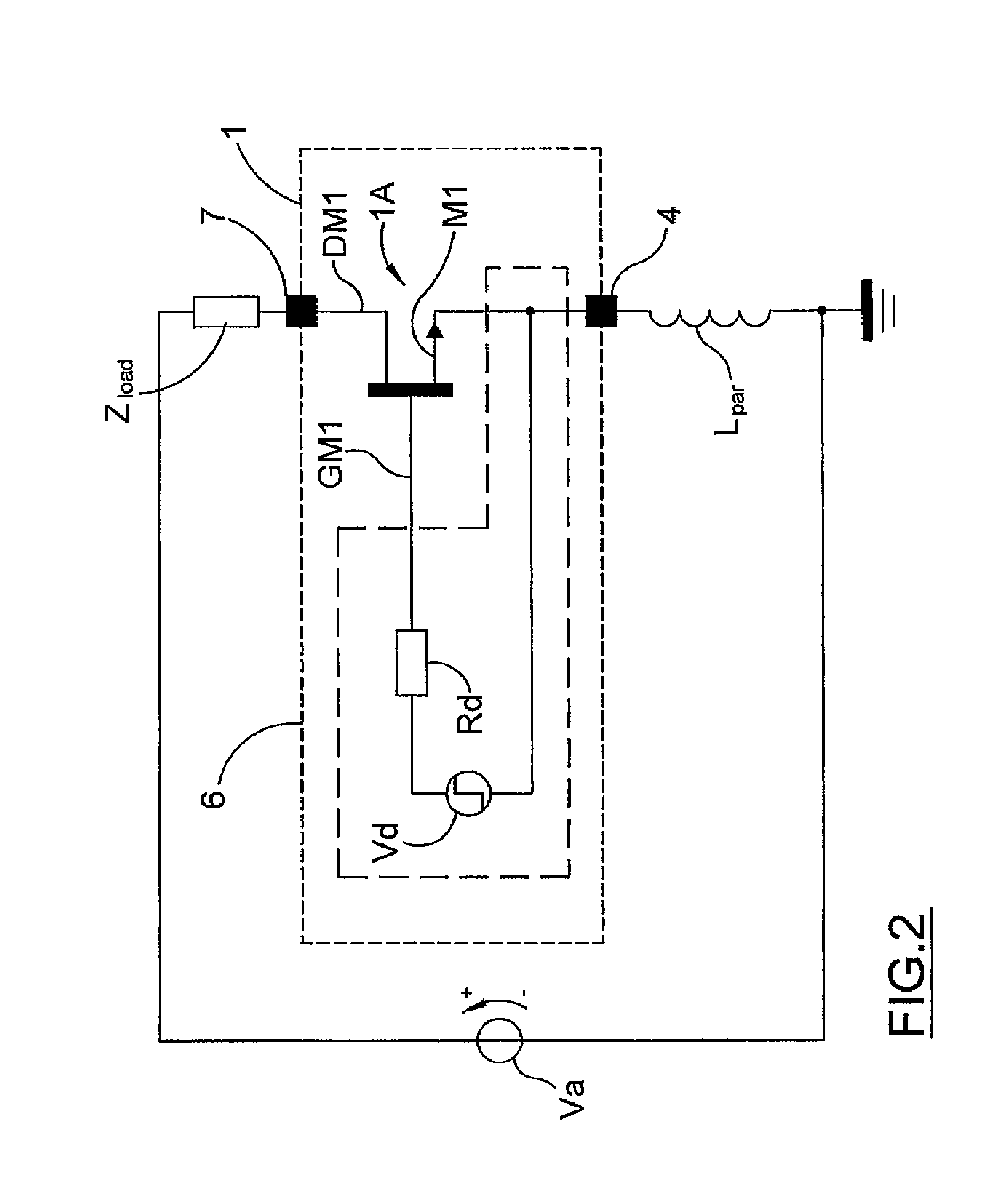
One known problem of power integrated circuits, that is susceptible of causing malfunctioning, is the inevitable parasitic inductance of connecting wires for connection of the integrated circuit with a package.
In real cases, the voltage VLpar may also be of considerable value, and this may lead to malfunctions of the integrated circuit 1, not excluding any irreparable damages thereto.
The drawback of this method is that the MOS transistor M1 is typically turned on in a fixed manner, without accounting for any changes in the parasitic inductance Lpar, for the features of the load Zload, and for the MOS transistor M1 itself.
Also, the voltage that drives the MOS transistor M1 cannot be simply “shaped” to adequately control the Lpardl / dt without using costly circuit arrangements.

Method used


Image

  • Power integrated circuit with high insensitivity to parasitic inductances of wires for connection to a package and package for said integrated circuit
  • Power integrated circuit with high insensitivity to parasitic inductances of wires for connection to a package and package for said integrated circuit
  • Power integrated circuit with high insensitivity to parasitic inductances of wires for connection to a package and package for said integrated circuit

Examples


first embodiment

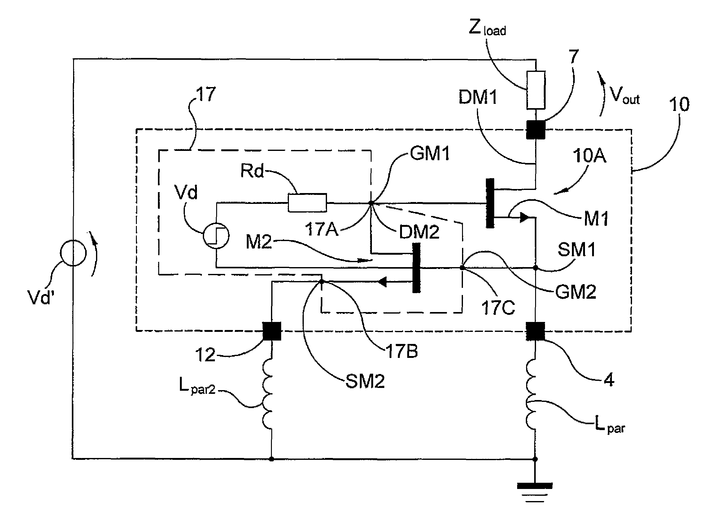
[0042]Referring initially to FIGS. 5A and 5B, which show the present disclosure, and to certain parts as mentioned above and designated with the same numerals, an integrated circuit 10 is shown to have a power output stage 10A which is driven by a driving stage or drive circuit 11.

[0043]The integrated circuit 10 further has at least one first pad 7, one second pad 4 and one third pad 12, other than said first 7 and said second pads 4.

[0044]Particularly, the drive circuit 11 is electrically coupled between the third pad 12 and said power output stage 10A.

[0045]It shall be noted, namely with reference to FIG. 5B, that the second pad 4 of the integrated circuit 19 is electrically coupled to a pin, e.g., the pin P7 of said plurality of pins P1-P10 of the package 2, and said third pad 12 of the integrated circuit 19 is also electrically coupled to said first pin, e.g., the pin P7, thereby generating a negative feedback that can control any potential difference between said third pad 7 an...

second embodiment

[0070]Referring now to FIG. 6, which shows the present disclosure, and to certain parts as mentioned above and designated with the same numerals, it can be noted that the output stage 10A comprises transistor means M1 having a gate terminal GM1, a drain terminal DM1, and a source terminal SM1, where the first pad 7 is electrically coupled to said drain terminal DM1 and the second pad 4 is electrically coupled to said source terminal SM1.

[0071]It can be further noted that the integrated circuit 10 comprises a drive circuit 17 having a first terminal 17A, a second terminal 17B and a third terminal 17C, where:[0072]the first terminal 17A is electrically coupled to said gate terminal GM1,[0073]the second terminal 17B is electrically coupled to said third pad 12 and[0074]the first terminal 17C is electrically coupled to said source terminal SM1.

[0075]Furthermore, the drive circuit 17 comprises voltage generator means Vd and resistor means Rd connected in series with each other and transi...

third embodiment

[0085]Referring now to FIG. 7, which shows the present disclosure, and to certain parts as mentioned above and designated with the same numerals, the integrated circuit 10 is shown to have a power output stage 10A with first power transistor means M1 having a gate terminal GM1, a drain terminal DM1 and a source terminal SM1.

[0086]The integrated circuit 10 has a first pad 7 electrically coupled to said drain terminal DM1 and a second pad 4 electrically coupled to said source terminal SM1.

[0087]The integrated circuit 10 further comprises a drive circuit 18 having a first terminal 18A, a second terminal 18B and a third terminal 17C, where:[0088]the first terminal 18A is electrically coupled to said gate terminal GM1,[0089]the second terminal 18B is electrically coupled to said third pad 12 and[0090]the third terminal 18C is electrically coupled to said drain terminal DM1.

[0091]The drive circuit 18 further comprises first voltage generator means Vd′ connected in series with first resist...


PUM


Abstract

The present disclosure relates to an integrated circuit and a package on which such integrated circuit is placed, the latter having a power output stage, at least one first pad, one second pad and one drive circuit for driving said power output stage, wherein the integrated circuit is characterized in that it has at least one additional third pad, other than said at least one first and said at least one second pads, said drive circuit being electrically coupled between said at least one third pad and said power output stage.

Description

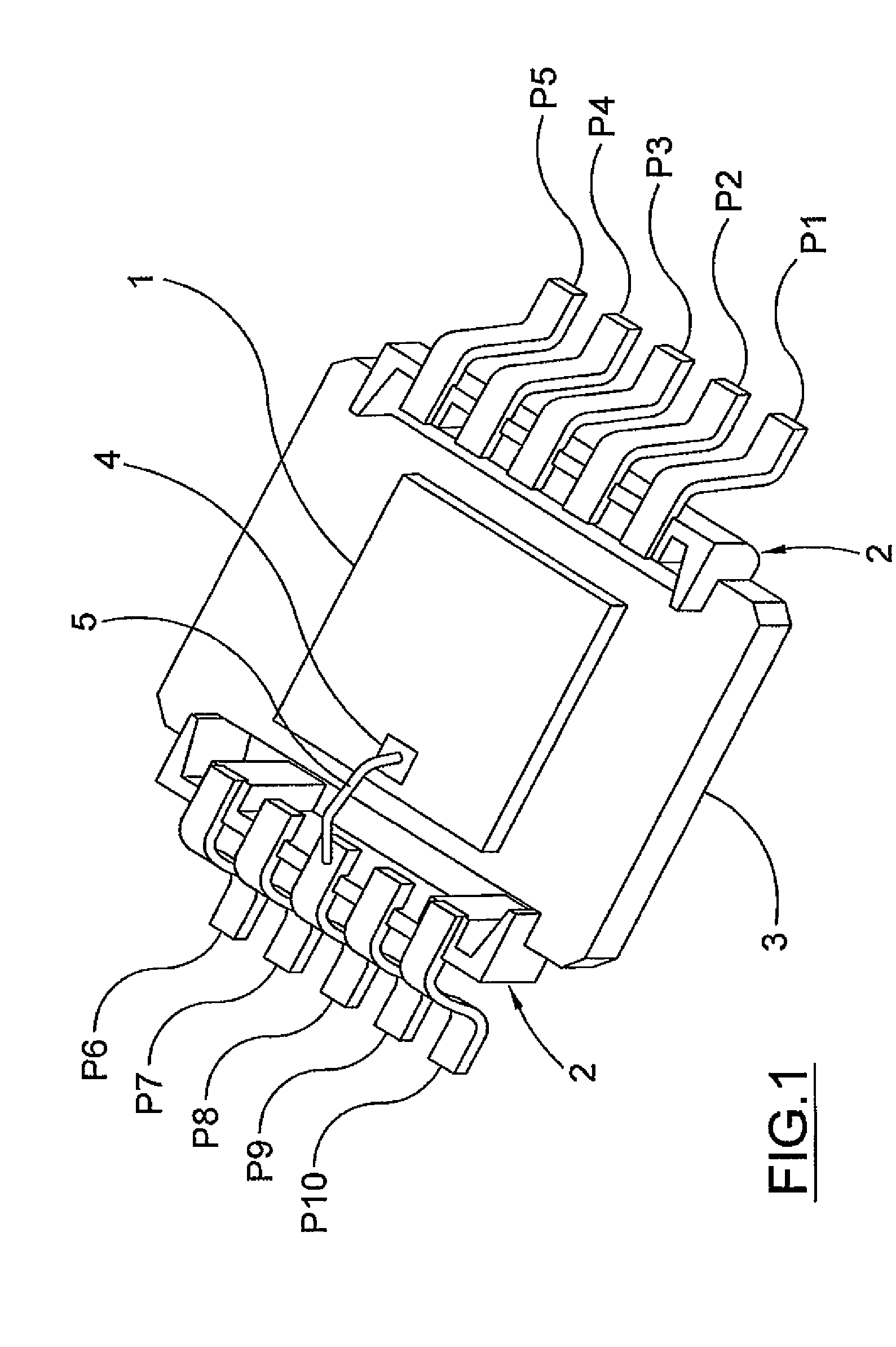
BACKGROUND[0001]1. Technical Field[0002]The present disclosure relates to an integrated power circuit and the package on which such integrated circuit is placed, and particularly, but without limitation, to a switching power integrated circuit with high insensitivity to parasitic inductances of the wires for connection with a package.[0003]2. Description of the Related Art[0004]One known problem of power integrated circuits, that is susceptible of causing malfunctioning, is the inevitable parasitic inductance of connecting wires for connection of the integrated circuit with a package.[0005]For example, with reference to FIG. 1, which shows a perspective view of a power integrated circuit 1 when placed on a package 2, the connection between the integrated circuit 1 and the package 2 is found to occur by means of one or more connection wires 5.[0006]Particularly, the integrated circuit 1 may be a MOSFET power transistor or an Insulated Gate Bipolar Transistor (IGBT), whereas the packa...

Claims


Application Information

Patent Timeline
Patent Type & Authority Patents(United States)
IPC IPC(8): H02H9/00
CPCH01L23/50H01L24/49H01L2924/1305H01L2224/48091H01L2224/48247H01L2224/49113H01L2924/01015H01L2924/01033H01L2924/01082H01L2924/13055H01L2924/13091H01L2924/14H01L2924/19042H01L2924/19043H01L2924/30107H01L2924/3011H01L24/48H01L2924/00014H01L2924/00H01L2224/05554H01L2924/10162H01L2224/45099H01L2224/05599
Inventor BOTTI, EDOARDOADDUCI, PIETRO MARIO
Owner STMICROELECTRONICS SRL
Learn More