Power MOSFET active gate drive based on negative feedback mechanism

a technology of negative feedback and active gate drive, which is applied in the direction of pulse generator, pulse manipulation, pulse technique, etc., can solve the problems of false trigger, additional switching loss, additional complexity, and reliability concerns due to extra components

Active Publication Date: 2022-05-17
BEIJING JIAOTONG UNIV +1
View PDF1 Cites 0 Cited by
  • Summary
  • Abstract
  • Description
  • Claims
  • Application Information

AI Technical Summary

Benefits of technology

[0044]The technical issue to be solved by the present invention is to provide a power MOSFET gate drive based on negative feedback mechanism, which can automatically suppress the induced gate voltage, or the so-called crosstalk, without sacrificing the switching speed and without increasing circuit complexity of a MOSFET.
[0055]The present invention has the following advantages. The negative feedback active gate drive (NFAGD) has a simple structure and easy to be realized using a conventional gate drive chip, a drive resistor, an auxiliary MOSFET and an auxiliary capacitor, without involving any additional logical circuits. Functionally, the negative feedback active gate drive (NFAGD) can automatically suppress the induced gate-source voltage and make the gate voltage of the MOSFET stable even during high-speed switching operation without sacrificing the switching speed of the MOSFET. In subsequent embodiments, compared to conventional passive suppression approaches, the negative feedback active gate drive (NFAGD) provides greater suppression of gate-source voltage spikes and oscillation. It can suppress the crosstalk without influencing the switching speed, thus enables coordinated optimization of gate voltage stability and switching behavior.

Problems solved by technology

Severe spikes and oscillations may lead to false triggers and additional switching losses, even lead to shooting thorough [9].
However, the complex auxiliary logic circuits are needed for detecting the induced gate voltage, or for predicting the variation trend of the induced gate voltage, to take preemptive action.
However, from the end-users' point of view, additional complexity is added along with the reliability concern due to extra components.
Thus, the acceptance and adoption of these advanced gate drive techniques are limited.
Moreover, due to the circuit propagation delay, the clamping bandwidth is not high enough for the crosstalk suppression [11, 21].
On the other hand, due to the high switching speed, the detected gate voltage is interfered with mainly by the common-source inductance between the drive loop and power loop, which is inevitable in practical situations [21].
AMC technique shows a significant crosstalk suppression with lower dv / dt ratings; However, some limitations and enlarged disturbance are visible at higher dv / dt, for example, higher than around 20 V / ns in the test bench used in the literature [11].
However, additional complexity is added along with the reliability concern due to extra components.
Thus, the acceptance and adoption of these advanced gate drive techniques are limited.
The prediction is not always accurate, especially in a fast switching condition, due to detection deviation, propagation delay and parasitic inductances.
High dv / dt and di / dt can result in crosstalk phenomenon with gate glitch, false-triggering, and other detrimental effects during switching transients.
Also, limited feedback control works focus on crosstalk suppression.
The implementation of negative feedback control in fast switching SiC and GaN devices for crosstalk suppression is challenging.
Firstly, considering the switching time for SiC and GaN devices is as short as tens of nanoseconds, the propagation delay of the feedback control is a concern since it may be comparable, even longer than the switching time.
Secondly, fast switching is always associated with parasitic ringing so that sensors that attempt to identify different switching subintervals easily interfere, resulting in improper operation.
However, coordinated optimization of gate voltage stability and switching speed is challenging.

Method used


Image

  • Power MOSFET active gate drive based on negative feedback mechanism
  • Power MOSFET active gate drive based on negative feedback mechanism
  • Power MOSFET active gate drive based on negative feedback mechanism

Examples


Embodiment Construction

[0074]One mode for implementing the present invention is now described.

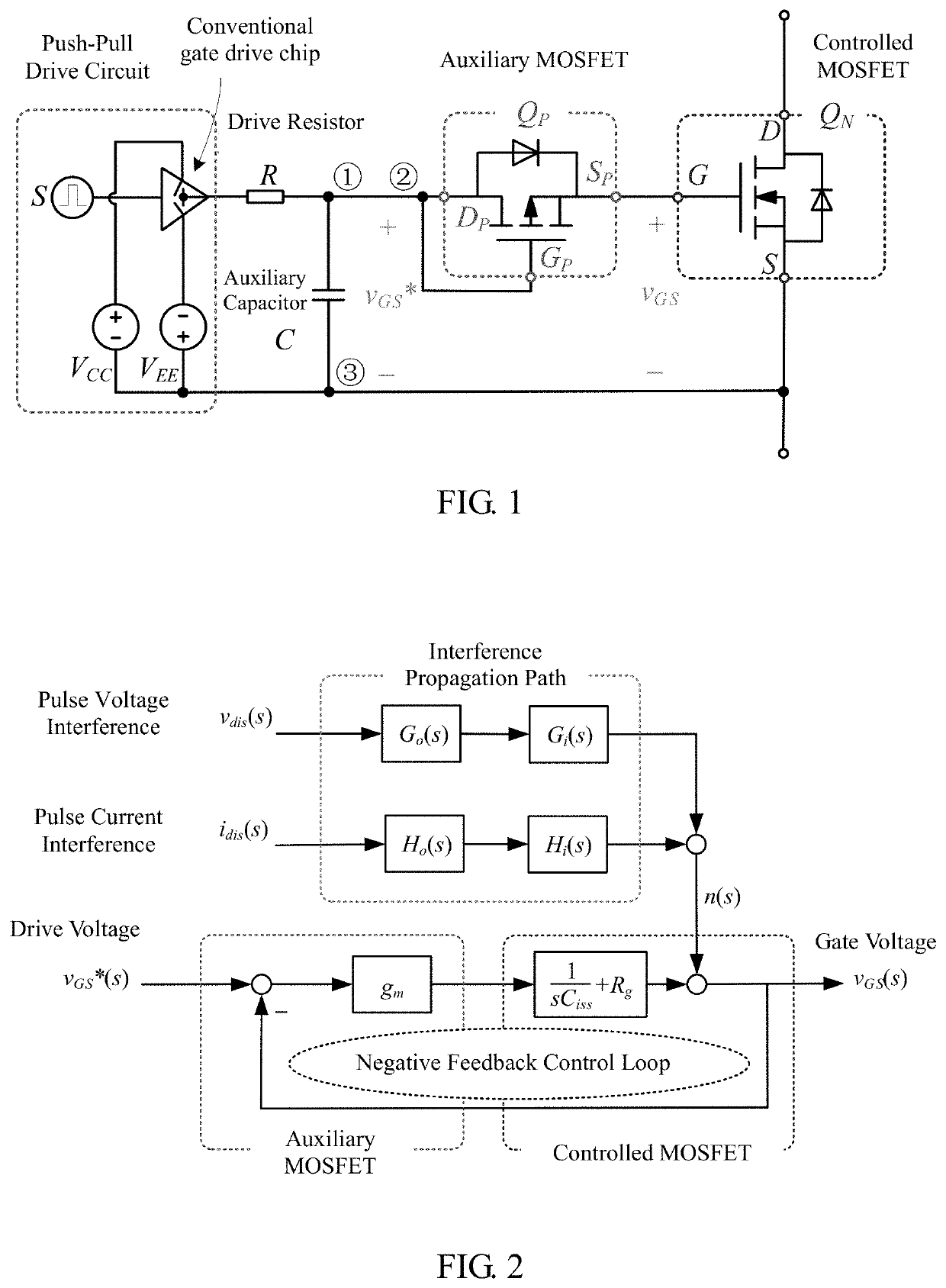
[0075]As shown in FIG. 1, a negative feedback active gate drive (NFAGD) is used to drive a MOSFET QN. The output of a conventional gate MOSFET drive is connected to a network, constituted by the drive resistor R and the auxiliary capacitor C. The output of the RC network is also regarded as the drive reference vGS*. It then goes to the gate and source of controlled MOSFET through the auxiliary MOSFET. For building the negative feedback, the controlled MOSFET and auxiliary MOSFET should have a complementary channel characteristic. Usually, the controlled MOSFET is N-channel. Hence the auxiliary MOSFET is P-channel. Hereafter, this invention denotes the controlled MOSFET and the auxiliary MOSFET as QN and QP. The RC network is responsible for tuning the speed of switching. The gate voltage vGS would follow the drive reference vGS*, owing to the negative feedback control. Hence the speed of gate voltage vGS is simil...


PUM

PropertyMeasurementUnit
internal gate resistanceaaaaaaaaaa
drain currentaaaaaaaaaa
drain-source voltageaaaaaaaaaa

Abstract

This invention introduces the negative feedback into the gate drive. It proposes a negative feedback active gate drive (NFAGD) for silicon carbide (SiC) and gallium nitride (GaN) semiconductor devices to fully utilize their potential of high switching-speed capability in a phase-leg configuration. An auxiliary P-channel MOSFET is introduced to construct a negative feedback control mechanism. Due to the negative feedback mechanism, the proposed drive can automatically attenuate the disturbance from the complementary device of the phase-leg. The negative feedback active gate drive (NFAGD) has a simple structure and easy to be realized using a push-pull drive circuit, a drive resistor, an auxiliary MOSFET and an auxiliary capacitor, without involving any additional logical circuits. Functionally, the negative feedback active gate drive (NFAGD) can automatically suppress the induced gate-source voltage and make the gate voltage of the MOSFET stable even during high-speed switching operation without sacrificing the switching speed of the MOSFET.

Description

BACKGROUND OF THE INVENTION1. Technical Field[0001]The present invention relates to an active gate drive circuit for a power MOSFET based on negative feedback mechanism.2. Description of Related Art[0002]The emergence of silicon carbide (SiC) and gallium nitride (GaN) semiconductor devices promises to revolutionize next-generation power electronics converters [1-4]. Compared with Si devices, SiC and GaN devices featured with high breakdown electric field, low on-state resistance, fast switching speed, and high junction temperature capability [5, 6]. These characteristics are beneficial for the efficiency, power density, and reliability of power electronics converters [7-9]. However, in a practical converter with phase-leg configuration, the switching transient of one device will impact its complementary device, generating the crosstalk phenomenon [4, 10].[0003]The crosstalk phenomenon is characterized by large high-frequency spikes and oscillations on the interfered device's gate vo...

Claims


Application Information

Patent Timeline
Patent Type & Authority Patents(United States)
IPC IPC(8): H03K3/00H03K5/00H03K17/687H03K17/10H01L29/20H01L29/16
CPCH03K17/102H01L29/1608H01L29/2003H03K17/687H02M1/32H02M1/08H02M1/0038H03K17/04123H03K17/162
Inventor SHAO, TIANCONGLI, ZHIJUNZHENG, TRILLION Q.HUANG, BOWANG, JUNXING
Owner BEIJING JIAOTONG UNIV
Why Eureka
Try Eureka