Semiconductor device enabling further microfabrication

a technology of semiconductor devices and microfabrication, applied in semiconductor devices, diodes, electrical devices, etc., can solve the problems of insufficient memory cell structure, difficult to create such contact, etc., and achieve the effect of satisfying the request for further microfabrication

Active Publication Date: 2012-04-24
LONGITUDE LICENSING LTD
View PDF5 Cites 7 Cited by
  • Summary
  • Abstract
  • Description
  • Claims
  • Application Information

AI Technical Summary

Benefits of technology

[0011]According to the semiconductor device or the method for manufacturing the semiconductor, the distance between a source electrode or a drain electrode and the wiring connected to the source electrode or to the drain electrode becomes closer, which results in easily forming a contact plug for connecting the source electrode or the drain electrode to the wiring. Therefore, further microfabrication can be implemented.

Problems solved by technology

Although there is increased demand for microfablication, it is difficult to create such a contact.
Furthermore, the memory cell structure proposed in Japanese Patent Laid-Open No. 2000-164833 is not sufficient to meet the request for further microfabrication.

Method used


Image

  • Semiconductor device enabling further microfabrication
  • Semiconductor device enabling further microfabrication
  • Semiconductor device enabling further microfabrication

Examples


first embodiment

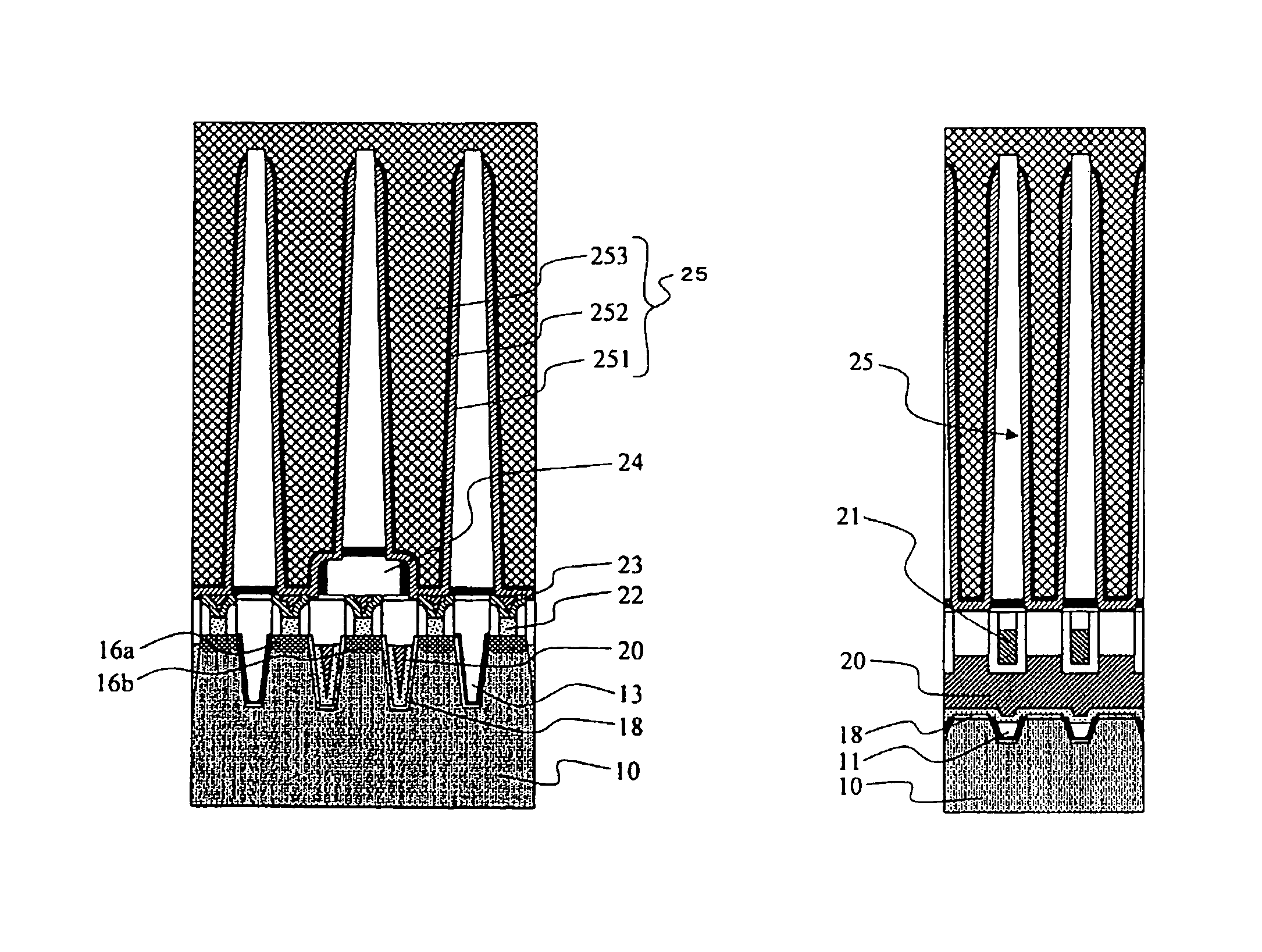
[0038]The DRAM memory cell structure in accordance with the present embodiment will be described.

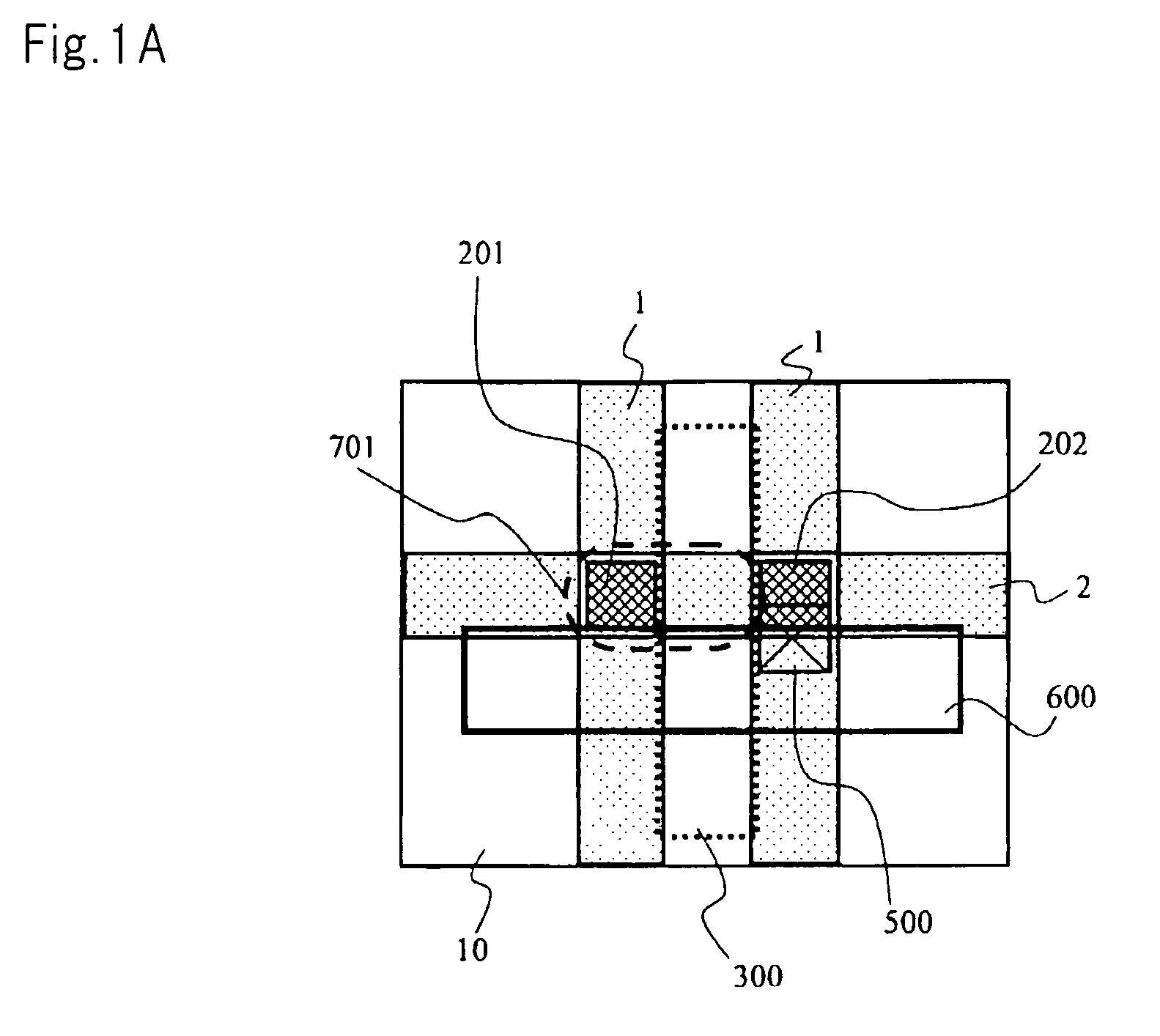
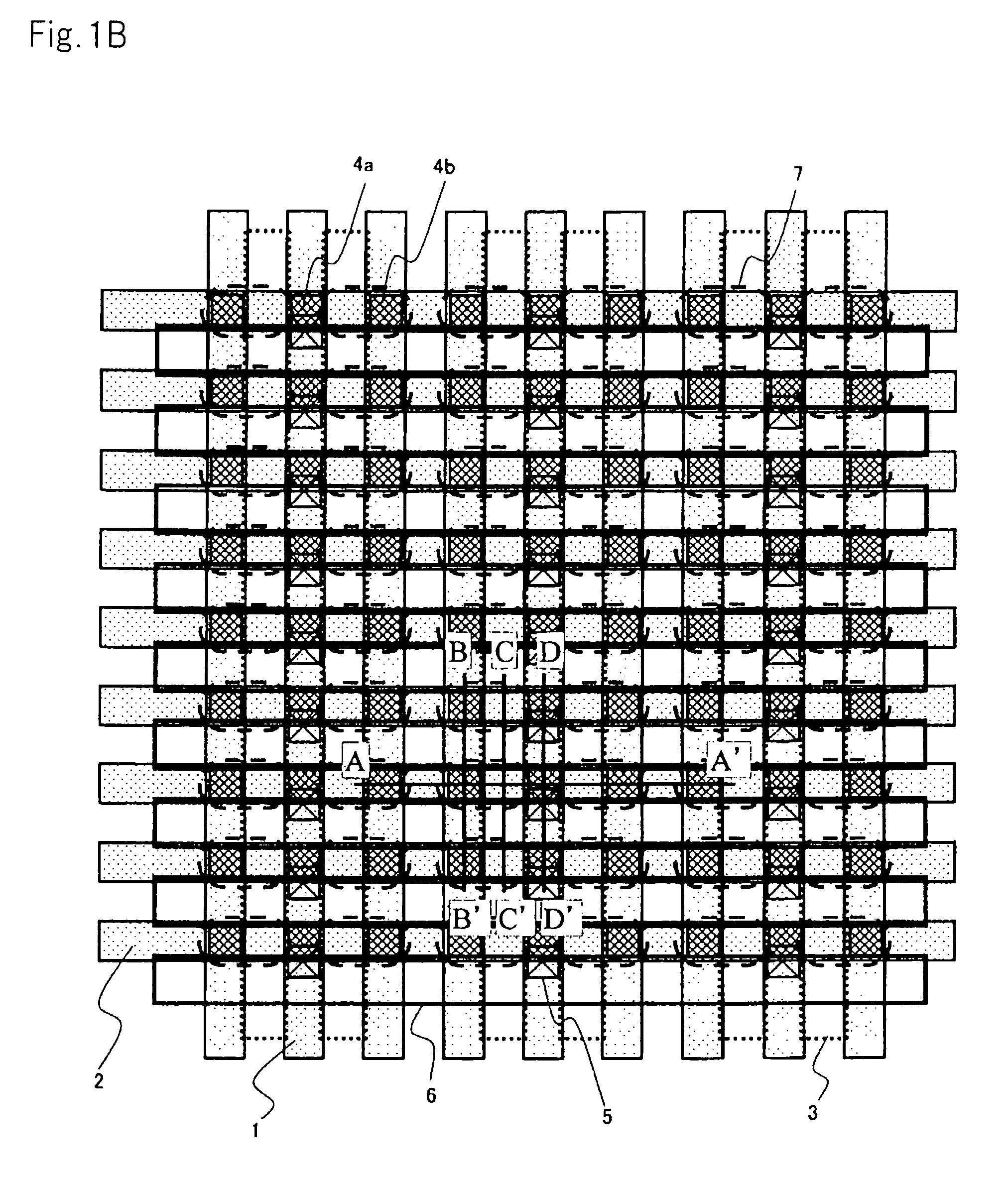
[0039]FIG. 1A is a plan view for explaining a memory cell pattern in accordance with the present embodiment. The memory cell of the present embodiment uses an open bit line architecture and has an area of 6F2, where F denotes a feature size which means a minimum process to be used. Moreover, the memory cell is formed on a semiconductor substrate made of silicon (hereinafter referred to as Si substrate).

[0040]The memory cell in accordance with the present embodiment is configured to have a capacitor for storing information and a MOS transistor connected to the capacitor. The MOS transistor functions as an access transistor serving to read information from the capacitor or to write information into the capacitor. Hereinafter, the MOS transistor of the memory cell is referred to as the access transistor.

[0041]As illustrated in FIG. 1A, the access transistor includes drain electrode 201 and ...

second embodiment

[0095]According to the present embodiment, the semiconductor device in accordance with the present invention is applied to a memory cell other than the DRAM.

[0096]According to the memory cell described in the first embodiment, instead of the capacitor element, a structure having a storage element using resistance change may be considered. The storage element using a change in resistance and the MOS transistor may be combined to form a memory cell such as a phase change memory (PRAM) and a resistive memory (ReRAM).

[0097]More specifically, in the case of phase change memory, the storage element, which includes a chalcogenide material (GeSbTe, etc.,) whose resistance changes with the phase change, may be formed instead of the capacitor element.

[0098]The method of manufacturing the semiconductor device in accordance with the present embodiment will be described with emphasis on only the processes that are different from the first embodiment.

[0099]In the same manner as in the first embod...


PUM


Abstract

A semiconductor device includes a plurality of MOS transistors and wiring connected to a source electrode or a drain electrode of the plurality of MOS transistors and, the wiring being provided in the same layer as the source electrode and the drain electrode in a substrate, or in a position deeper than a surface of the substrate.

Description

[0001]This application is based upon and claims the benefit of priority from Japanese Patent Application No. 2008-174605 filed on Jul. 3, 2008, the content of which is incorporated by reference.BACKGROUND OF THE INVENTION[0002]1. Field of the Invention[0003]The present invention relates to a semiconductor device having a MOS (Metal Oxide Semiconductor) transistor and a method for manufacturing the same.[0004]2. Description of Related Art[0005]A DRAM (Dynamic Random Access Memory) is a device having a plurality of memory cells which combine a MOS transistor and a storage element serving as a capacitor. In a general memory cell, a gate electrode of the MOS transistor is formed on a silicon (Si) substrate. A line connecting the gate electrodes of the adjacent memory cells is called a word line.[0006]Japanese Patent Laid-Open No. 2000-164833 has proposed a memory cell having a structure in which a word line is provided inside the substrate unlike a general memory cell structure. The dis...

Claims


Application Information

Patent Timeline
Patent Type & Authority Patents(United States)
IPC IPC(8): H01L27/108
CPCH01L21/823418H01L21/823475H01L27/0629H01L27/24H01L29/66621H10B63/00
Inventor UCHIYAMA, HIROYUKI
Owner LONGITUDE LICENSING LTD
Why Eureka
Try Eureka