Radio-frequency module

a radio frequency module and module technology, applied in the field of radio frequency modules, can solve the problems of increasing loss in signal transfer, difficult to meet the recent demand for radio frequency amplifier circuits with high, and generating heat by hbt, so as to improve the characteristic of heat released, close the distance between the semiconductor device and the output matching circuit, and close the effect of heat releas

Pending Publication Date: 2022-06-16
MURATA MFG CO LTD
View PDF0 Cites 2 Cited by
  • Summary
  • Abstract
  • Description
  • Claims
  • Application Information

AI Technical Summary

Benefits of technology

[0006]To implement radio-frequency amplifier circuits with high power output, it is desirable to improve the characteristic of heat released from a semiconductor device including, for example, an HBT. It is difficult to satisfy recent demand for radio-frequency amplifier circuits with high power output by using the radio-frequency module disclosed in U.S. Patent Application Publication No. 2015 / 0303971. Additionally, when the operating frequency is relatively high, loss in signal transfer tends to increase. Accordingly, the present disclosure provides a radio-frequency module capable of suppressing increases in signal transfer loss and also improving the characteristic of heat released from a semiconductor device.
[0008]The second member including the radio-frequency amplifier circuit is joined to the first member including the band selection switch, and consequently, the radio-frequency module can be smaller than if the radio-frequency amplifier circuit and the band selection switch are individually mounted on or in the module substrate. Two heat transfer paths are formed; one is a heat transfer path from the semiconductor element included in the radio-frequency amplifier circuit to the first member; and the other is a heat transfer path from the semiconductor element to the module substrate via the conductive protrusion. As a result, it is possible to improve the characteristic of heat released from the semiconductor element included in the radio-frequency amplifier circuit.
[0009]No circuit component except the components constituting the output matching circuit is disposed between the passive element included in the output matching circuit and the semiconductor device in plan view, or the passive element constituting the output matching circuit overlaps the semiconductor device in plan view. As a result, it is possible to close the distance between the semiconductor device and the output matching circuit. Consequently, it is possible to close the distance from each of the radio-frequency amplifier circuit and the band selection switch that are disposed in the semiconductor device to the output matching circuit. Because this shortens the transfer line from the radio-frequency amplifier circuit to the output matching circuit and the transfer line from the output matching circuit to the band selection switch, it is possible to reduce transfer loss.

Problems solved by technology

While an HBT operates, the HBT generates heat because collector dissipation occurs.
It is difficult to satisfy recent demand for radio-frequency amplifier circuits with high power output by using the radio-frequency module disclosed in U.S. Patent Application Publication No. 2015 / 0303971.
Additionally, when the operating frequency is relatively high, loss in signal transfer tends to increase.

Method used


Image

  • Radio-frequency module
  • Radio-frequency module
  • Radio-frequency module

Examples


first embodiment

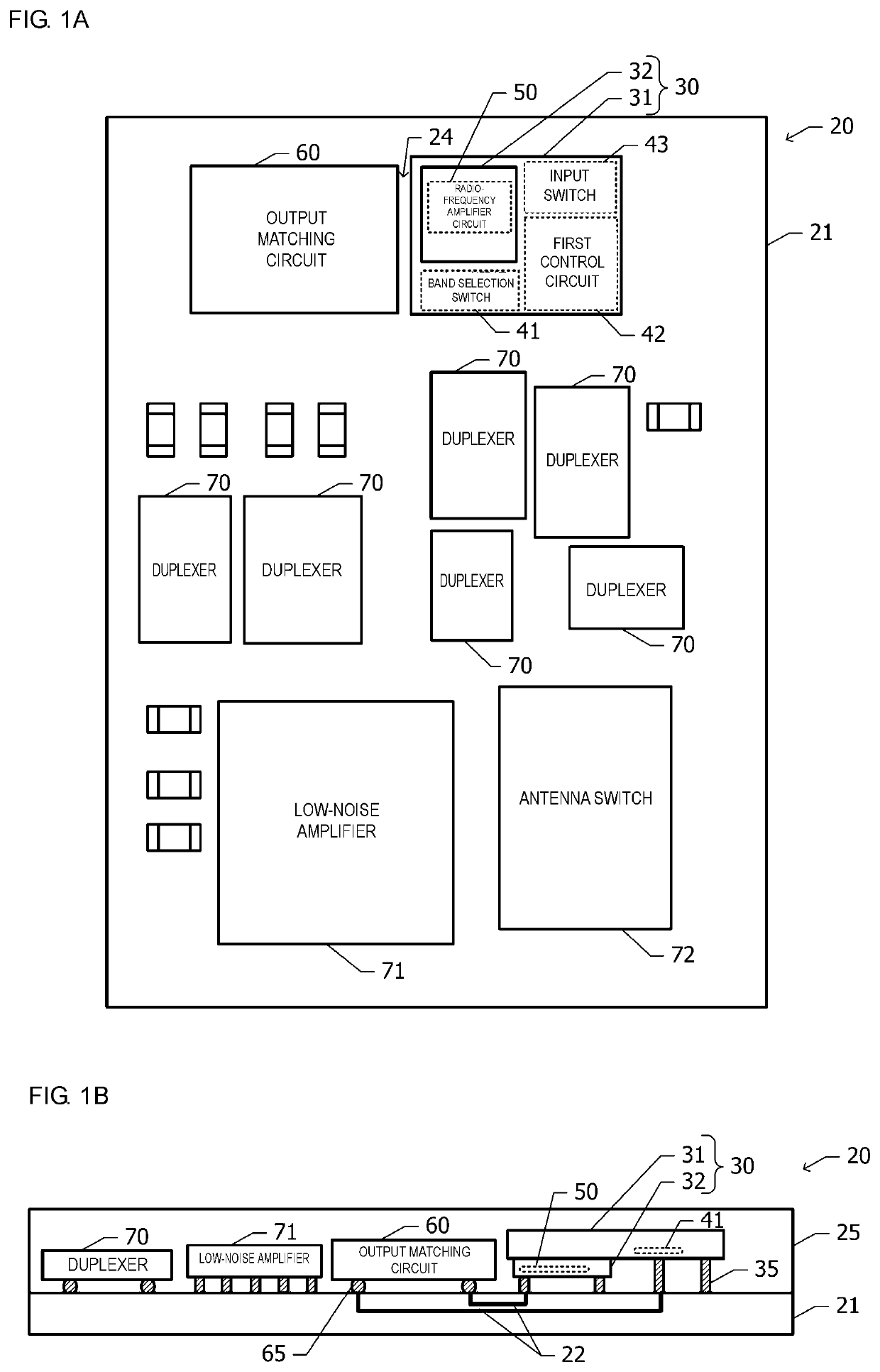
[0026]A radio-frequency module according to a first embodiment will be described with reference to drawings in FIGS. 1A to 5D.

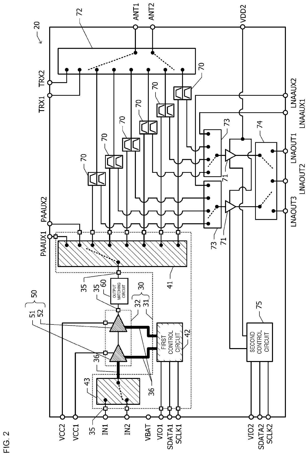
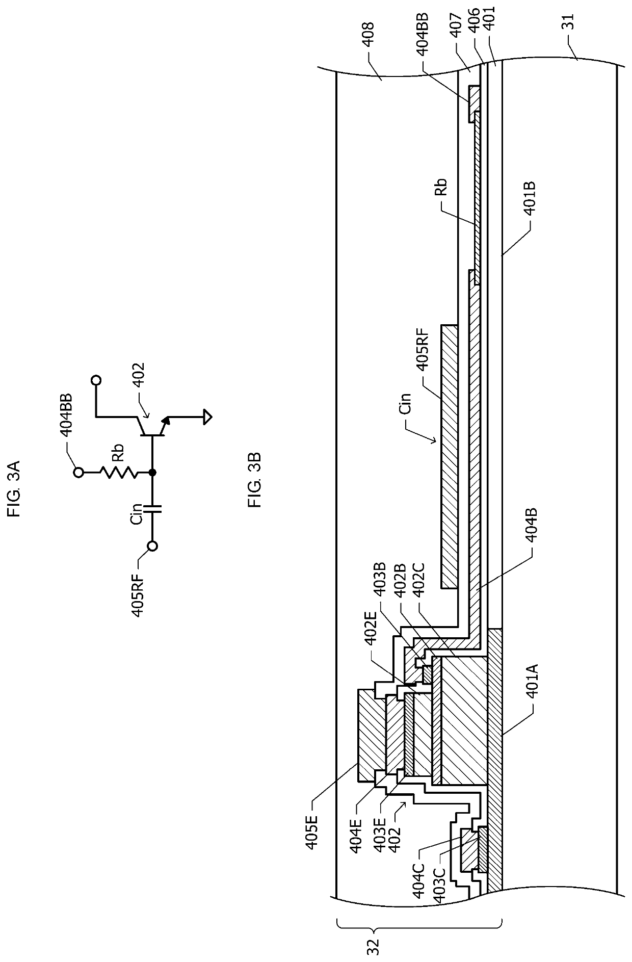
[0027]FIG. 1A illustrates an arrangement of constituent elements of a radio-frequency module 20 according to the first embodiment in plan view. FIG. 1B schematically illustrates a sectional structure of the radio-frequency module 20. On a module substrate 21, a semiconductor device 30, an output matching circuit 60, a plurality of duplexers 70, a low-noise amplifier 71, an antenna switch 72, and other surface-mount passive elements (surface-mount devices (SMDs)) are mounted. The semiconductor device 30 includes a first member 31 and a second member 32 joined to the first member 31 in surface contact with the first member 31. The first member 31 may be made of, for example, an elemental semiconductor. The second member 32 may be made of, for example, a compound semiconductor.

[0028]A band selection switch 41, a first control circuit 42, and an input switch 43 a...

second embodiment

[0077]Next, a radio-frequency module according to a second embodiment will be described with reference to FIGS. 6A to 7B. The following description does not repeat configurations common to the radio-frequency module according to the first embodiment described with reference to FIGS. 1A to 5D.

[0078]FIG. 6A illustrates an arrangement of constituent elements of the radio-frequency module 20 according to the second embodiment in plan view. FIG. 6B schematically illustrates a sectional structure of the radio-frequency module 20. In the first embodiment (FIG. 1A), the semiconductor device 30 does not overlap the output matching circuit 60 in plan view, but the semiconductor device 30 is disposed in close proximity to the output matching circuit 60. By contrast, in the second embodiment, the semiconductor device 30 overlaps at least a portion of one or some passive elements of the plurality of passive elements included in the output matching circuit 60 in plan view.

[0079]As illustrated in ...

third embodiment

[0087]Next, a radio-frequency module according to a third embodiment will be described with reference to FIGS. 8A and 8B. The following description does not repeat configurations common to the radio-frequency module according to the second embodiment described with reference to FIGS. 6A to 7B.

[0088]FIG. 8A is an equivalent circuit diagram illustrating an example of the output matching circuit 60. A single-ended amplifier circuit is used as the radio-frequency amplifier circuit 50 in the second embodiment, but a differential amplifier circuit is used as the radio-frequency amplifier circuit 50 in the third embodiment. The radio-frequency amplifier circuit 50 has two output ports for outputting differential signals. The output matching circuit 60 includes an output transformer having a primary coil L5 and a secondary coil L6, a ground-connected capacitor C5, and a series-connected capacitor C6.

[0089]The primary coil L5 of the output transformer is coupled between the two output ports....


PUM

PropertyMeasurementUnit
radio-frequencyaaaaaaaaaa
frequencyaaaaaaaaaa
temperatureaaaaaaaaaa

Abstract

A semiconductor device including a radio-frequency amplifier circuit and a band selection switch is mounted on or in a module substrate. An output matching circuit coupled between the radio-frequency amplifier circuit and the band selection switch is on or in the module substrate. The semiconductor device includes a first member at which the band selection switch having a semiconductor element made of an elemental semiconductor is formed and a second member joined to the first member in surface contact therewith. The radio-frequency amplifier circuit including a semiconductor element made of a compound semiconductor is formed at the second member. Conductive protrusions are raised from first and second members. The semiconductor device is mounted on or in the module substrate with the conductive protrusions interposed therebetween, and in plan view, is in close proximity to the output matching circuit or overlaps a passive element constituting the output matching circuit.

Description

CROSS-REFERENCE TO RELATED APPLICATION[0001]This application claims benefit of priority to Japanese Patent Application No. 2020-205984, filed Dec. 11, 2020, the entire content of which is incorporated herein by reference.BACKGROUNDTechnical Field[0002]The present disclosure relates to a radio-frequency module.Background Art[0003]Radio-frequency (RF) front-end modules capable of both transmitting and receiving radio-frequency signals are installed in electronic devices for communications such as mobile communications and satellite communications. An RF front-end module includes, for example, a monolithic microwave integrated circuit (MMIC) capable of amplifying radio-frequency signals, a control integrated circuit (IC) for controlling a radio-frequency amplifier circuit, a switch IC, and a duplexer.[0004]U.S. Patent Application Publication No. 2015 / 0303971 discloses a radio-frequency module miniaturized by stacking a control IC on an MMIC. The radio-frequency module disclosed in U.S....

Claims


Application Information

Patent Timeline
Patent Type & Authority Applications(United States)
IPC IPC(8): H01L23/66H01L25/16H01L23/367H03F3/195H04B1/44
CPCH01L23/66H01L25/16H01L23/367H03F3/195H03F2200/451H01L2223/6611H01L2223/665H01L2223/6655H01L2223/6672H04B1/44H04B1/40H01L23/49811H01L23/5389H01L23/538H03F1/56H03F2200/108H03F2200/301H01L2924/15192H01L2924/19105H01L2224/16227H01L2924/19011H01L2924/19041H01L2924/19042H01L2224/32145H01L2224/73253H01L2224/81815H01L2224/131H01L2224/13147H01L2224/13144H01L2224/13082H01L2223/6688H01L2924/19106H01L2224/16235H01L2224/94H01L24/11H01L24/13H01L24/16H01L24/81H03F3/245H03F3/72H03F2203/7209H03F2200/294H03F2200/111H01L2924/014H01L2924/00014H01L2224/03H01L2224/11
Inventor YOSHIMI, SHUNJISAMATA, MITSUNORI
Owner MURATA MFG CO LTD
Why Eureka
Try Eureka