Multi-layer distributed network

a distributed network and multi-layer technology, applied in the field of clock/buffer network, can solve the problems of increasing the difficulty of routing test signals in these devices, increasing the difficulty of routing, and increasing the complexity of routing, so as to reduce current leakage

Active Publication Date: 2012-04-24
ALTERA CORP
View PDF11 Cites 0 Cited by
  • Summary
  • Abstract
  • Description
  • Claims
  • Application Information

AI Technical Summary

Benefits of technology

[0009]In another aspect of the present invention, a process for preparing an integrated circuit is disclosed. A network is created in the process. The network may include a center network that branches into quadrants on the integrated circuit. The center network transmits test signals from test pins on the integrated circuit to each of the different quadrants. Each of the quadrants has a quadrant network that is connected to the cen

Problems solved by technology

However, intensive test signal routing may cause congestion in the device, especially if the device is configured for a fairly complex application.
As devices become smaller with more complex circuitry to support a wide variety of features, routing test signals in these devices has become more challenging.
In other words, routing has become more complicated because the routing area has shrunk while the number of test signals has i

Method used


Image

  • Multi-layer distributed network
  • Multi-layer distributed network
  • Multi-layer distributed network

Examples


Embodiment Construction

[0020]The following embodiments describe integrated circuits and a process for distributing test signals in an integrated circuit. It will be obvious, however, to one skilled in the art, that the present invention may be practiced without some or all of these specific details. Also, some embodiments of the invention are described in the context of programmable logic devices, a type of integrated circuit, but the invention is not limited to programmable logic devices. Further, well-known operations have not been described in detail in order not to unnecessarily obscure the described embodiments of the present invention.

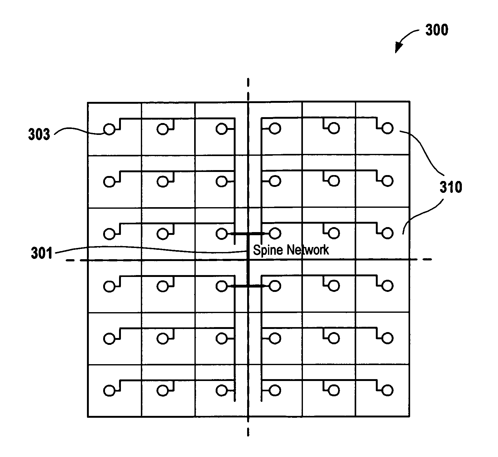
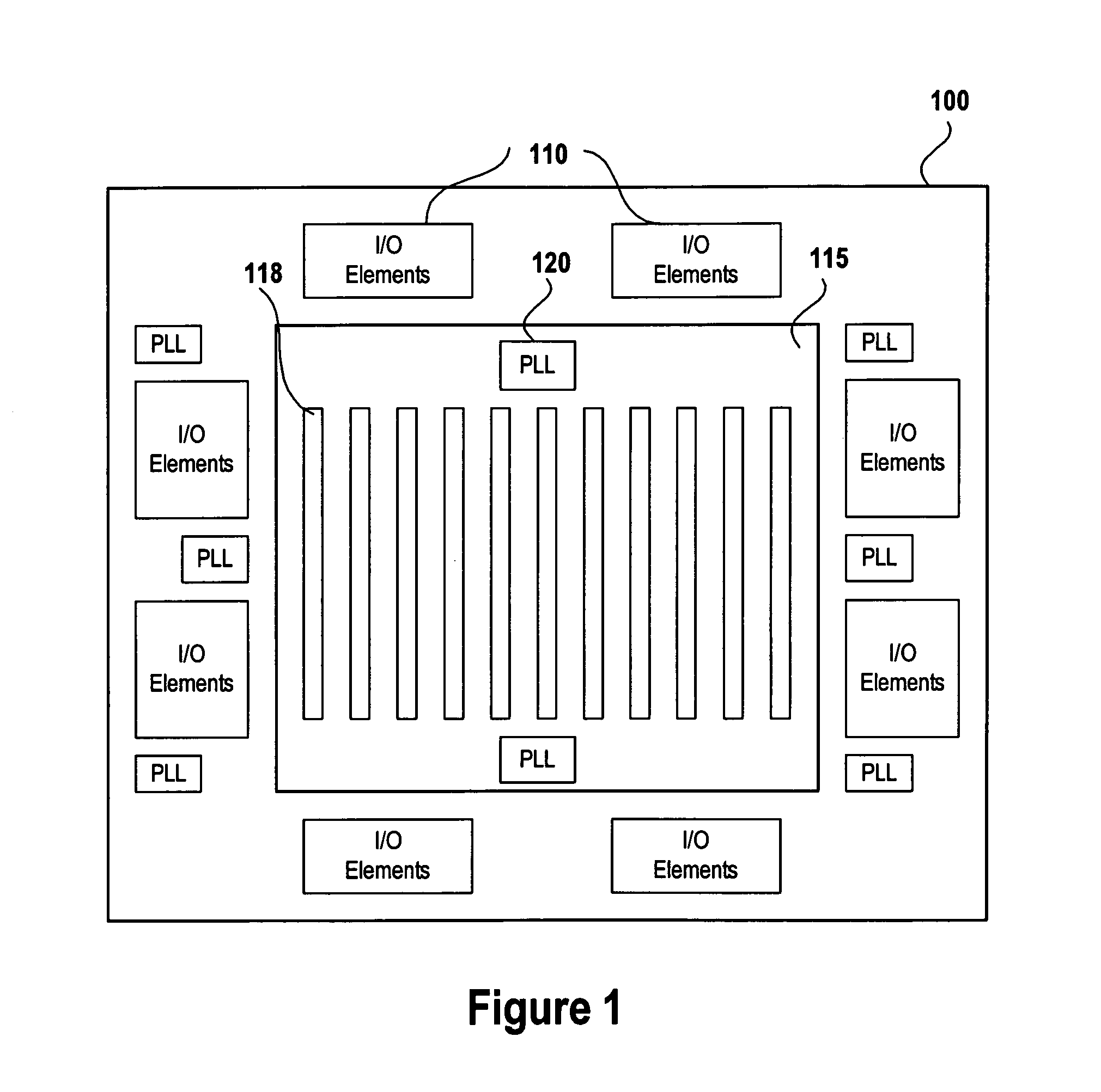
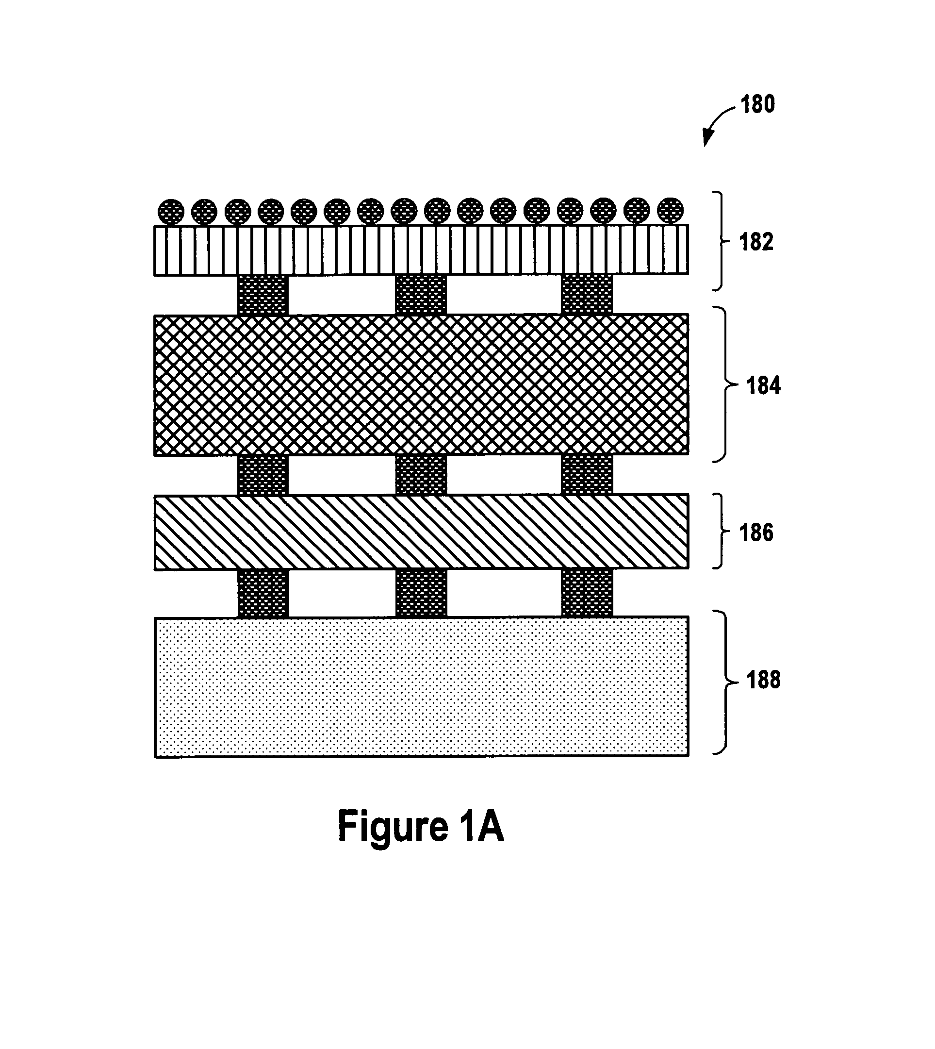
[0021]Embodiments described herein provide techniques for routing test signals in an integrated circuit without creating routing congestion in the circuit. Certain types of programmable devices, such as a mask-programmable logic device, have different metallization layers, some of which are customizable while others are non-customizable. Customizable layers or custom l...


PUM


Abstract

Apparatuses and processes for distributing signals in an integrated circuit are disclosed. An embodiment to use a custom layer together with a base layer on an integrated circuit for testing the integrated circuit includes having a structured network on the base layer. The custom layer connects the network to logic elements on the integrated circuit. The network may be evenly distributed across the base layer of the integrated circuit. Even distribution of the network may reduce skew of the test signals. Buffers are also placed along the structured network. The buffers may be placed to ensure a deterministic test signals distribution. Unused buffers in the base layer may be tied off to reduce current leakage.

Description

BACKGROUNDDescription of the Related Art[0001]The present invention relates generally to a clock / buffer network in an integrated circuit device. More specifically, the invention relates to test signal routing in a device with a pre-built network in a non-customizable metal layer and an auto-routing network in a customizable metal layer.[0002]Integrated circuit devices are used in a wide array of applications. To verify the quality of these devices, numerous tests can be carried out. Each device can be put through a rigorous industry standard test methodology to verify the quality of the device. Different test signals are typically controlled by different test pins and all these signals are routed to different parts of the integrated circuit to fully test the functionality of the circuit. As such, test signals need to be routed to different blocks in the integrated circuit to test the functionality of each logic block in an integrated circuit.[0003]However, intensive test signal rout...

Claims


Application Information

Patent Timeline
IPC IPC(8): G06F17/50
CPCG06F17/505G06F17/5054G06F2217/14G06F2217/62G06F2217/84G06F13/40G06F30/34G06F30/333G06F30/327G06F30/396G06F2119/12G06F30/347
Inventor OH, KEONG HONGTAN, YEE LIANGLOH, SIANG POHLIM, CHOOI PEI
Owner ALTERA CORP
Why Eureka
Try Eureka