Check patentability & draft patents in minutes with Patsnap Eureka AI!

Semiconductor device and method of manufacturing the same

a semiconductor device and semiconductor technology, applied in the field of semiconductor devices, can solve problems such as the degradation of the yield of semiconductor devices, and achieve the effects of high yield, reduced short circuiting and bleeding, and uniform fillet geometry

Inactive Publication Date: 2012-05-08
RENESAS ELECTRONICS CORP
View PDF11 Cites 5 Cited by
  • Summary
  • Abstract
  • Description
  • Claims
  • Application Information

AI Technical Summary

Benefits of technology

The solution effectively suppresses inter-bump short circuiting and improves yield by enhancing the wettability and cleanability of the surface, preventing residue and bubble formation, and maintaining the integrity of the underfill material within the gap.

Problems solved by technology

In addition, the underfill material sometimes ran out from the gap between the semiconductor chip 126 and the solder resist film 118 in the process of filling, which could inhibit uniform formation of an underfill fillet, could cause bleeding, and could degrade yield of the semiconductor device.

Method used


Image

  • Semiconductor device and method of manufacturing the same
  • Semiconductor device and method of manufacturing the same
  • Semiconductor device and method of manufacturing the same

Examples


example 1

[0091]The semiconductor device shown in FIG. 2B and FIG. 3 was manufactured according to the conditions described below.

(a) Materials

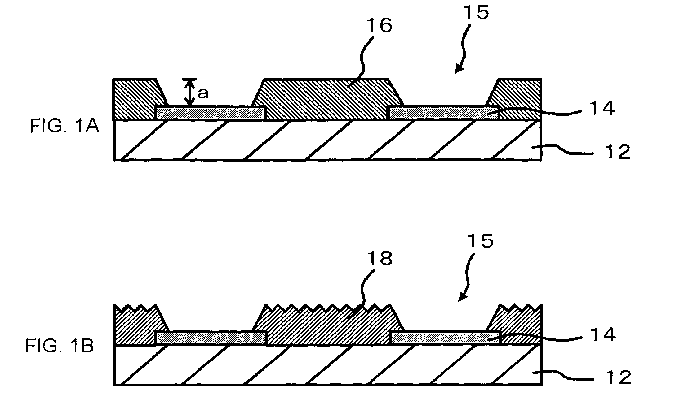
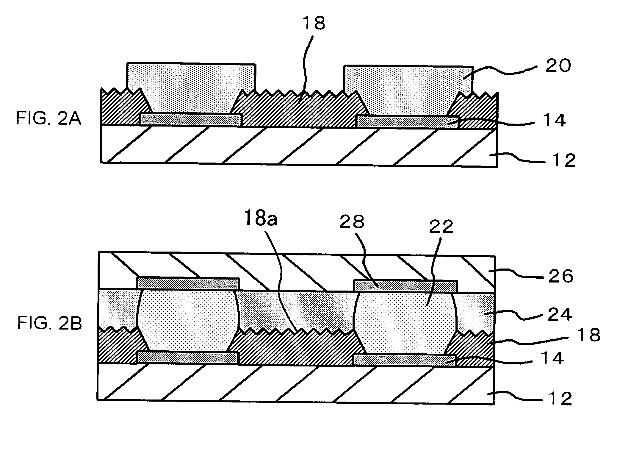
[0092]Solder resist film 18: epoxy resin film, PFR-800 AUS410 from Taiyo Ink MFG Co., Ltd.

[0093]Underfill film 24: epoxy-base resin; and

[0094]Bumps 22: lead-free solder.

(b) Roughening (Wet Blasting) of Surface of Solder Resist Film 18)

[0095]Using a wet blasting apparatus provided with a wide spray gun having an 1-mm-wide slit (product name: Physical Fine Etcher, from Macoho Co., Ltd.), and using A#800 alumina abrasive, wet blasting was carried out while setting the distance between the spray gun and the solder resist film 16 to approximately 10 mm to 30 mm, the air supply pressure to approximately 0.18 MPa to 0.25 MPa, and the process speed to approximately 1.0 m / min to 1.8 m / min.

(c) Method of Measuring Surface Roughness

[0096]Surface roughness Ra (arithmetical mean roughness) was measured using an atomic force microscope.

[0097]The surface roughness Ra ...

example 2

[0098]The semiconductor device was manufactured similarly to as described in Example 1, except that the wet blasting of the surface of the solder resist film 18 was carried out while adjusting the air supply pressure to approximately 0.25 MPa to 0.30 MPa.

[0099]The surface roughness Ra of the solder resist film 18 was found to be 0.5 μm.

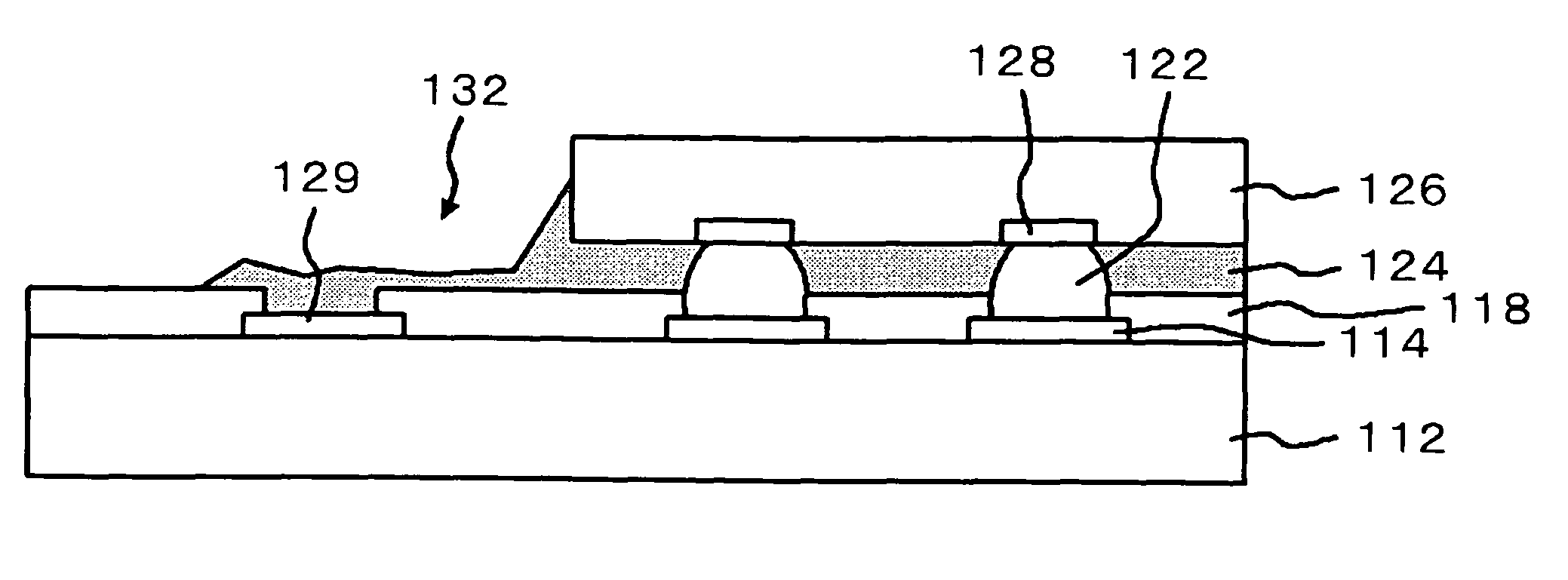
[0100]It was confirmed that the semiconductor device obtained in Examples 1, 2 were suppressed in the production of voids in the underfill film 24, and in the inter-bump short circuiting. It was also confirmed that the fillet geometry 32 of the underfill film 24 was settled in a predetermined geometry as shown in FIG. 3, leaving the second mounting pads provided around the semiconductor chip 26 exposed.


PUM


Abstract

Provided is a semiconductor device having a substrate, a semiconductor chip flip-chip mounted on the substrate, and a stacked film provided in a gap between the substrate and the semiconductor chip. The stacked film is composed of a protective film covering the surface of the substrate, and an underfill film formed between the solder resist film and the semiconductor chip. The protective film is roughened on the contact surface brought into contacting said underfill film.

Description

[0001]This application is based on Japanese patent application No. 2007-266808 the content of which is incorporated hereinto by reference.BACKGROUND[0002]1. Technical Field[0003]The present invention relates to a semiconductor device having an underfill filled in a gap between a semiconductor chip and a substrate, and a method of manufacturing the same.[0004]2. Related Art[0005]There has been known a conventional printed wiring board described in Japanese Laid-Open Patent Publication No. 2006-93493. The publication describes a printed wiring board having an insulating substrate provided with a protective layer roughened on the surface thereof using a buff or wet blasting, and an insulating base (prepreg) stacked on the protective layer. A film composed of epoxy acrylate resin is used for the protective layer.[0006]The publication describes that such configuration can improve adhesiveness between the protective layer and the insulating base.[0007]Japanese Laid-Open Patent Publication...

Claims


Application Information

Patent Timeline
Patent Type & Authority Patents(United States)
IPC IPC(8): H01L23/48
CPCH01L21/563H01L23/3142H01L25/105H01L23/49816H01L24/16H01L24/81H01L2224/73203H01L2224/73204H01L2224/81193H01L2224/81801H01L2924/15311H01L2924/1532H01L2924/15331H01L2225/1023H01L2225/1058H01L2224/16225H01L2224/32225H01L2924/00H01L2224/05571H01L2224/05573H01L2924/00014H01L2224/05599
Inventor ISHIDO, KIMINORI
Owner RENESAS ELECTRONICS CORP
Features
  • R&D
  • Intellectual Property
  • Life Sciences
  • Materials
  • Tech Scout
  • Unparalleled Data Quality
  • Higher Quality Content
  • 60% Fewer Hallucinations
Learn More