Semiconductor device and fabricating method thereof

a technology of semiconductor devices and semiconductor pads, applied in semiconductor devices, semiconductor/solid-state device details, electrical apparatus, etc., can solve problems such as metal giving rise, potential difference corrosion at the interfaces between wires and bond pads, etc., to prevent galvanic corrosion and reduce the number of defects in the first bond pads

Active Publication Date: 2012-05-22
AMKOR TECH SINGAPORE HLDG PTE LTD
View PDF4 Cites 12 Cited by
  • Summary
  • Abstract
  • Description
  • Claims
  • Application Information

AI Technical Summary

Benefits of technology

[0008]A semiconductor device is provided. The semiconductor device comprises a semiconductor die having bond pads, each of which consists of a first bond pad made of a material whose ionization tendency is relatively low and a second bond pad made of a material whose ionization tendency is relatively high. The second bond pads function as sacrificial anodes to prevent the occurrence of galvanic corrosion at the interfaces between the first bond pads and conductive wires. In an embodiment, the upper surfaces of the second bond pads are marked instead of those of the first bond pads, which reduces the number of defects in the first bond pads. A method for fabricating the semiconductor device is also provided.

Problems solved by technology

The use of the different metals gives rise to a potential difference between the wires and the bond pads.
As a result, the wires having a noble potential tend to corrode at a reduced rate and the bond pads having an active potential tend to corrode at an accelerated rate, resulting in corrosion at the interfaces between the wires and the bond pads.
Galvanic corrosion weakens the bonding between the conductive wires and the semiconductor die.
That is, galvanic corrosion is considered to be a major factor that causes disconnection of the conductive wires from the semiconductor die, resulting in operational failure or malfunction of the semiconductor device.
According to these methods, however, galvanic corrosion between wires and bond pads becomes a more serious problem during heating for the solidification of the FOWs.

Method used


Image

  • Semiconductor device and fabricating method thereof
  • Semiconductor device and fabricating method thereof
  • Semiconductor device and fabricating method thereof

Examples


Embodiment Construction

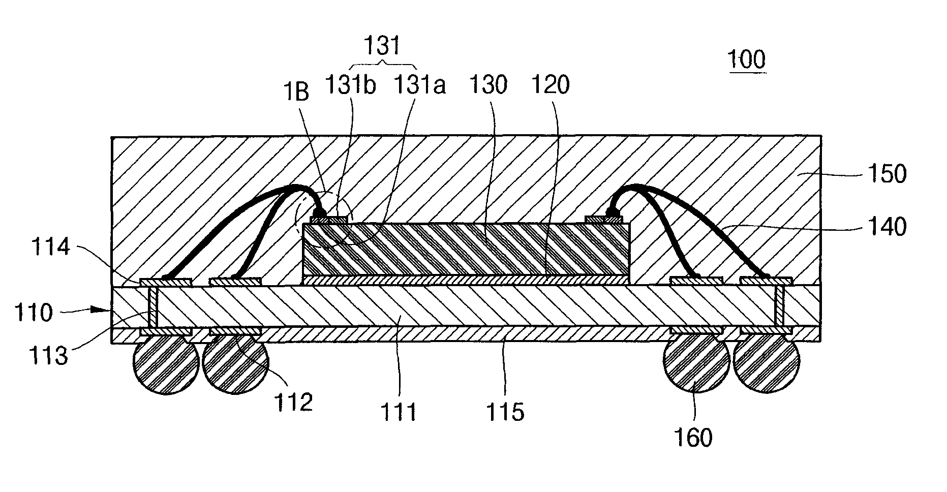
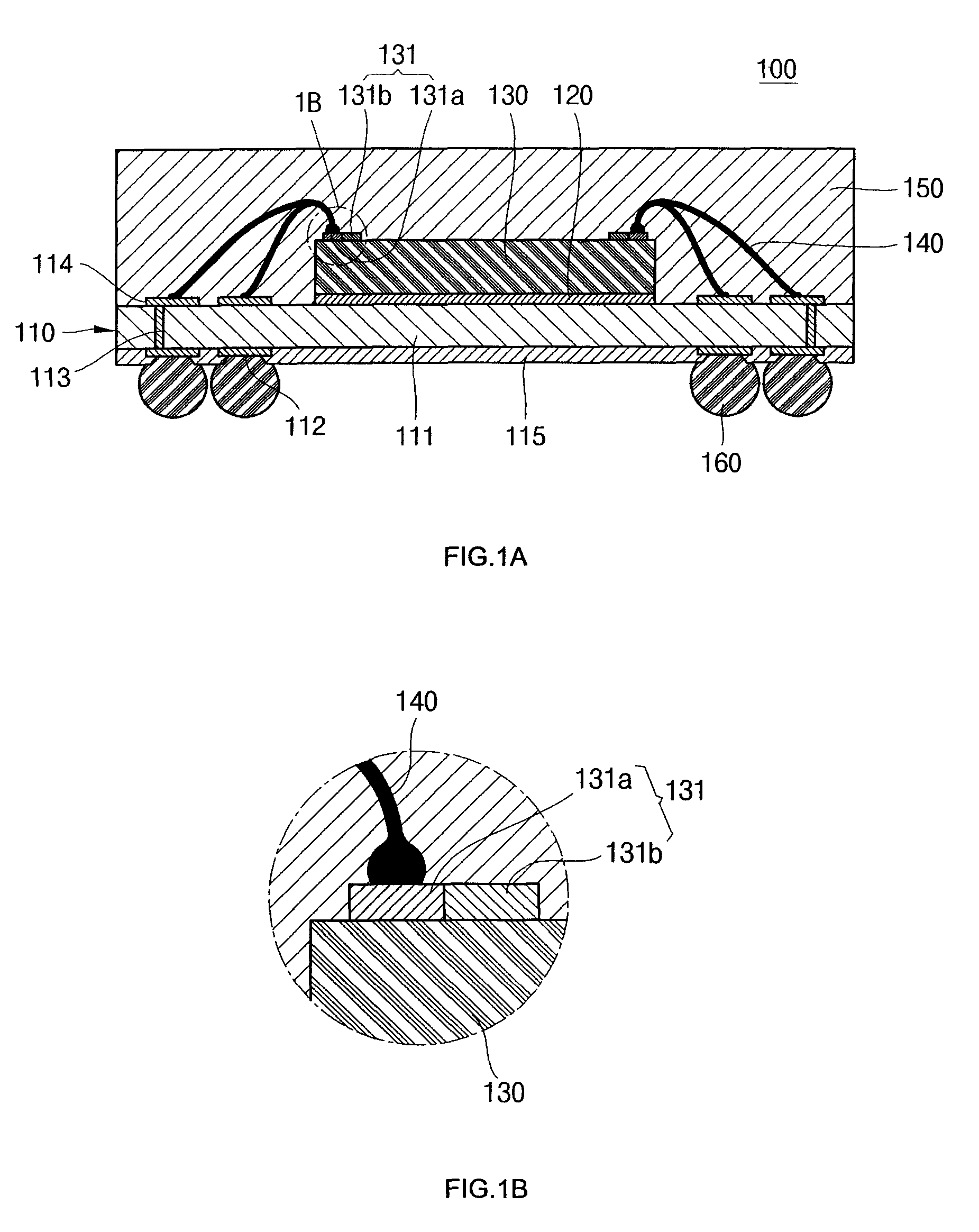
[0021]Referring to FIG. 1A, there is illustrated a cross-sectional view of a semiconductor device 100 according to an embodiment of the present invention. Referring to FIG. 1B, there is illustrated an enlarged view of area 1B of FIG. 1A. Referring to FIG. 1C, there is illustrated a plan view of a semiconductor die 130 used in the semiconductor device 100 according to the embodiment of the present invention.

[0022]As illustrated in FIGS. 1A through 1C, the semiconductor die 100 comprises a substrate 110, a semiconductor die 130 attached to the upper surface of the substrate 110, conductive wires 140 electrically connecting the substrate 110 to the semiconductor die 130, and an encapsulant 150 formed surrounding the semiconductor die 130. The semiconductor device 100 may further comprise solder balls 160 formed under the substrate 110.

[0023]The substrate 110 provides a base for the fabrication of the semiconductor device 110. The substrate 110 includes an insulating layer 111, lands 11...


PUM

PropertyMeasurementUnit
conductiveaaaaaaaaaa
depthaaaaaaaaaa
corrosionaaaaaaaaaa

Abstract

A semiconductor device is provided. The semiconductor device comprises a semiconductor die having bond pads, each of which consists of a first bond pad made of a material whose ionization tendency is relatively low and a second bond pad made of a material whose ionization tendency is relatively high. The second bond pads function as sacrificial anodes to prevent the occurrence of galvanic corrosion at the interfaces between the first bond pads and conductive wires. In an embodiment, the upper surfaces of the second bond pads are marked instead of those of the first bond pads, which reduces the number of defects in the first bond pads. A method for fabricating the semiconductor device is also provided.

Description

BACKGROUND OF THE INVENTION[0001]1. Field of the Invention[0002]The present invention relates to a semiconductor device and a method for fabricating the same.[0003]2. Description of the Related Art[0004]A typical semiconductor device has a structure in which conductive patterns of a substrate are interconnected to pads of a semiconductor die attached to the upper surface of the substrate through wires.[0005]The wires are made of gold or copper and the bond pads are made of aluminum. The use of the different metals gives rise to a potential difference between the wires and the bond pads. This potential difference allows electrons to migrate between the wires and the bond pads. As a result, the wires having a noble potential tend to corrode at a reduced rate and the bond pads having an active potential tend to corrode at an accelerated rate, resulting in corrosion at the interfaces between the wires and the bond pads. This corrosion is called “galvanic corrosion.”[0006]Galvanic corros...

Claims


Application Information

Patent Timeline
Patent Type & Authority Patents(United States)
IPC IPC(8): H01L23/488
CPCH01L24/05H01L25/0657H01L24/03H01L23/3128H01L2224/05556H01L24/29H01L24/32H01L24/45H01L24/85H01L2224/05578H01L2224/05601H01L2224/05618H01L2224/05623H01L2224/05624H01L2224/05638H01L2224/2919H01L2224/32145H01L2224/32225H01L2224/45139H01L2224/45144H01L2224/45147H01L2224/48091H01L2224/48227H01L2224/48465H01L2224/73265H01L2224/92247H01L2225/0651H01L2225/06565H01L2924/01012H01L2924/01013H01L2924/01029H01L2924/0103H01L2924/01079H01L2924/01082H01L2924/014H01L2924/15311H01L2924/01033H01L2924/01047H01L2924/0105H01L2224/85H01L2224/48624H01L2224/48618H01L2224/48623H01L2924/01014H01L2224/04042H01L2924/00014H01L2924/01048H01L2924/01004H01L2924/0665H01L2924/00012H01L2224/48824H01L2924/00H01L2224/48638H01L24/48H01L24/73H01L2224/02163H01L2224/48801H01L2224/48818H01L2224/48823H01L2224/48838H01L2924/14H01L2924/181
Inventor KIM, JOON SUPARK, JUNG SOOHWANG, TAE KYUNG
Owner AMKOR TECH SINGAPORE HLDG PTE LTD
Why Eureka
Try Eureka