Analog multiplexer configured to reduce kickback perturbation in image sensor readout

an analog multiplexer and readout technology, applied in the field of electronic circuitry, can solve the problems of affecting the proper operation of low-speed pgas, and affecting the readout performance of image sensors, so as to reduce or eliminate kickback perturbations and improve image sensor readout performance.

Active Publication Date: 2012-05-22
OMNIVISION TECH INC
View PDF4 Cites 4 Cited by
  • Summary
  • Abstract
  • Description
  • Claims
  • Application Information

AI Technical Summary

Benefits of technology

[0005]Illustrative embodiments of the invention provide an analog multiplexer for facilitating high-speed readout of an image sensor.
[0010]The illustrative embodiments advantageously reduce or eliminate kickback perturbations attributable to input switching of high-speed channel elements such as PGAs or DACs, thereby improving image sensor readout performance.

Problems solved by technology

Unfortunately, significant problems can arise when multiplexing several low-speed analog channels into a single high-speed analog channel.
For example, input switching operations associated with the high-speed PGA may disrupt the proper operation of the low-speed PGAs.
Conventional analog multiplexers are unable to provide an adequate solution to these problems.

Method used


Image

  • Analog multiplexer configured to reduce kickback perturbation in image sensor readout
  • Analog multiplexer configured to reduce kickback perturbation in image sensor readout
  • Analog multiplexer configured to reduce kickback perturbation in image sensor readout

Examples


Embodiment Construction

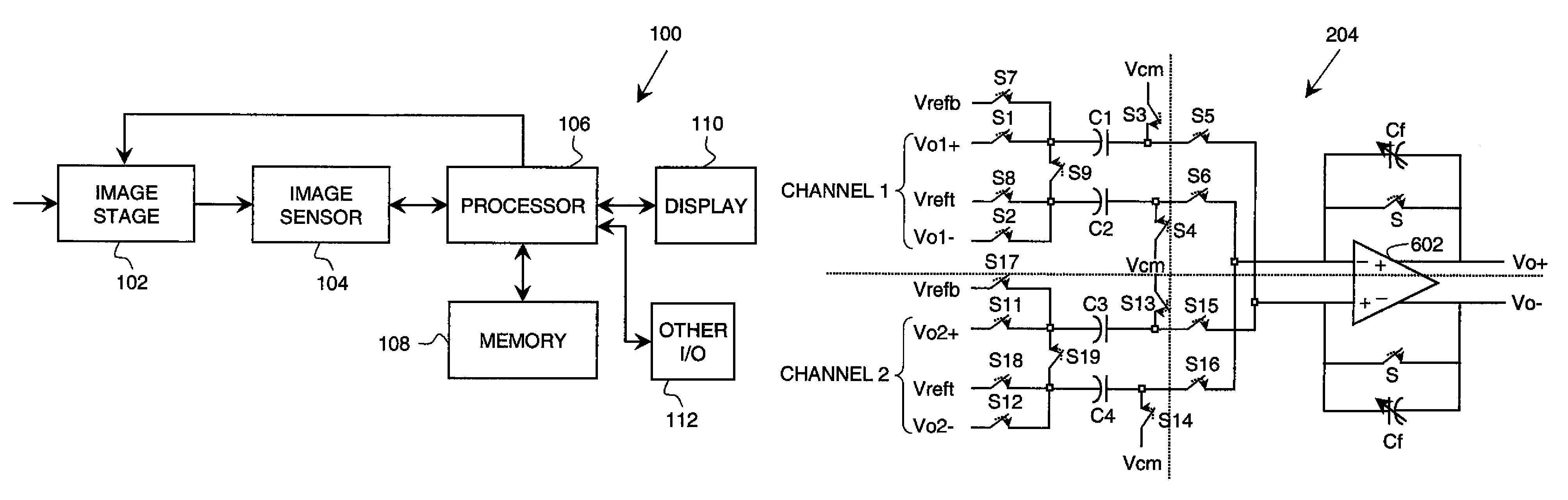
[0021]The present invention will be illustrated herein in conjunction with particular embodiments of digital cameras, image sensors and associated readout circuitry. It should be understood, however, that these illustrative arrangements are presented by way of example only, and should not be viewed as limiting the scope of the invention in any way. Those skilled in the art will recognize that the disclosed arrangements can be adapted in a straightforward manner for use with a wide variety of other types of imaging devices, image sensors and associated readout circuitry. Moreover, the analog multiplexing techniques of the invention can be implemented in applications other than those involving image sensor readout.

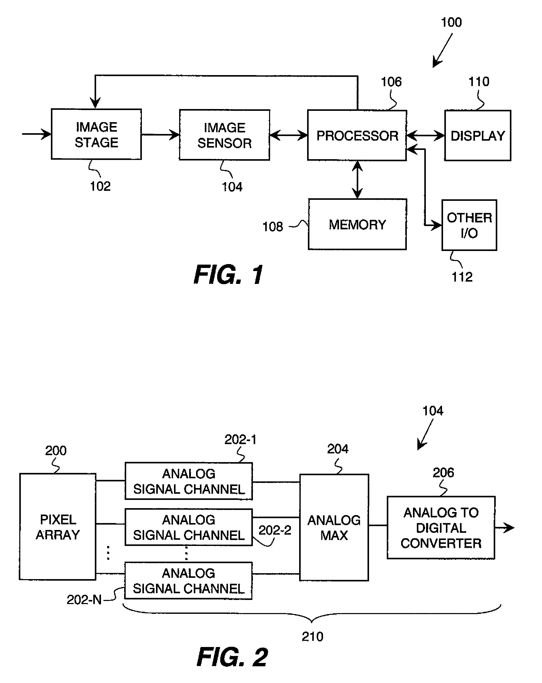
[0022]FIG. 1 shows a digital camera 100 in an illustrative embodiment of the invention. In the digital camera, light from a subject scene is input to an imaging stage 102. The imaging stage may comprise conventional elements such as a lens, a neutral density filter, an iris ...


PUM


Abstract

An analog multiplexer is configured to multiplex a plurality of input analog signal channels into a single output analog signal channel. The analog multiplexer comprises a plurality of input sampling circuits associated with respective ones of the input analog signal channels and an amplifier having an input controllably connectable in turn to each of the input sampling circuits. The analog multiplexer is further configured to connect at least a given one of the input analog signal channels to a sampling element of its corresponding input sampling circuit at a predetermined time prior to connecting the sampling element of that input sampling circuit to the input of the amplifier. The predetermined time is less than a full clock cycle of a sampling clock of the amplifier. The analog multiplexer may be implemented in readout circuitry coupled to a pixel array in an image sensor.

Description

FIELD OF THE INVENTION[0001]The present invention relates generally to electronic circuitry, and more particularly to analog multiplexing circuitry that may be used, for example, in conjunction with image sensor readout in digital cameras and other types of imaging devices.BACKGROUND OF THE INVENTION[0002]A typical electronic image sensor comprises a number of photodiodes or other photosensitive elements arranged in a two-dimensional array. These elements are also commonly referred to as picture elements or “pixels” and the corresponding array is referred to as a pixel array. Light incident on the pixel array is converted to electrical charge by the photosensitive elements. Collected electrical charge for a given image capture period is read from the photosensitive elements of the pixel array using an active pixel sensor (APS) or charge-coupled device (CCD) arrangement[0003]In order to read out the pixel array at high speed, it is often necessary to share certain signal processing c...

Claims


Application Information

Patent Timeline
Patent Type & Authority Patents(United States)
IPC IPC(8): H04N3/14
CPCH04N5/335H04N5/378H04N25/00H04N25/75
Inventor XUE, SONG
Owner OMNIVISION TECH INC
Why Eureka
Try Eureka