Charge gradient microscopy

a charge gradient and microscopy technology, applied in the field of scanning probe microscopy, can solve the problems of affecting the efficiency of pfm techniques, requiring expensive hardware, and limited data acquisition speed, and achieve the effect of more efficient approaches

Active Publication Date: 2015-10-22
UCHICAGO ARGONNE LLC
View PDF4 Cites 6 Cited by
  • Summary
  • Abstract
  • Description
  • Claims
  • Application Information

AI Technical Summary

Benefits of technology

[0006]Embodiments of the present invention provide devices and methods for high-speed imaging of ferroelectric and piezoelectric domains at the nanoscale. Such devices and methods allow for imaging to be carried out that is at least one or two orders of magnitude faster than conv...

Problems solved by technology

However, one of the major drawbacks of PFM is that the speed of data acquisition is limited by the resonance frequency of the cantilever of the PFM test apparatus and the time constant of the lock-in amplifier.
To acquire images at relatively higher frequencies, advanced lock-in equipment and specialized, expensive hardware are nee...

Method used


Image

  • Charge gradient microscopy
  • Charge gradient microscopy
  • Charge gradient microscopy

Examples


Embodiment Construction

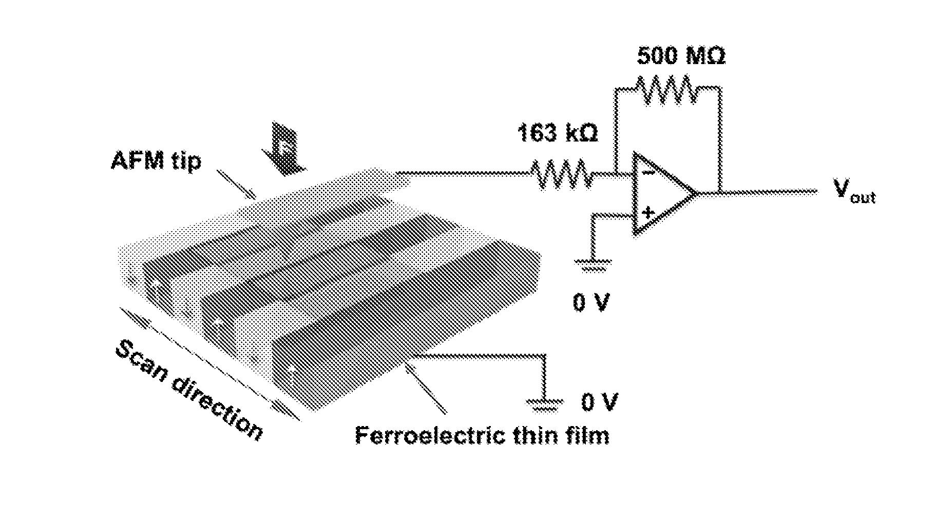
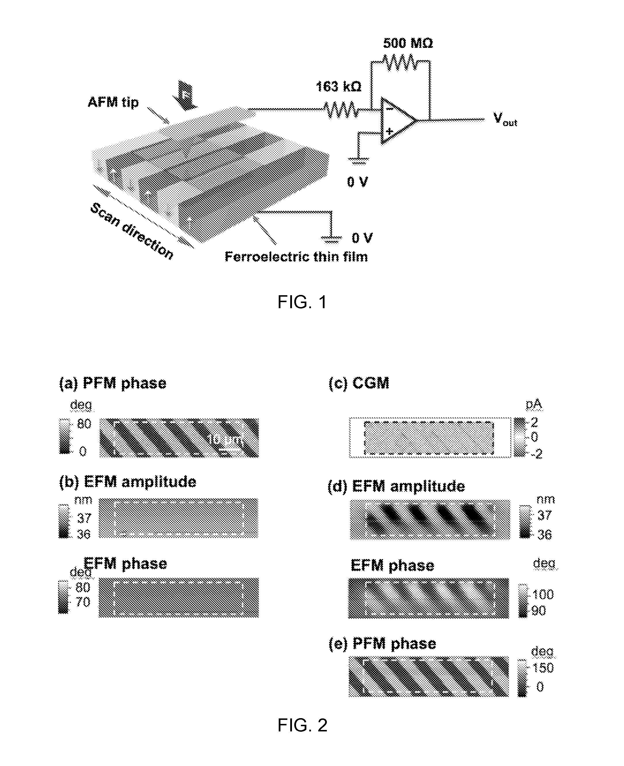
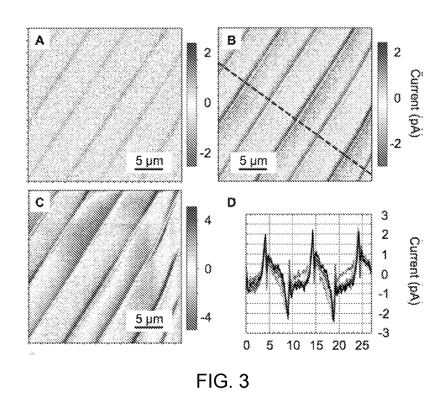
[0029]In the following detailed description, reference is made to the accompanying figures, which form a part hereof. In the figures, similar symbols typically identify similar elements, unless context dictates otherwise. The illustrative embodiments described in the detailed description, figures, and claims are not meant to be limiting. Other embodiments may be utilized, and other changes may be made, without departing from the spirit or scope of the subject matter presented here. It will be readily understood that the aspects of the present disclosure, as generally described herein, and illustrated in the figures, can be performed, arranged, substituted, combined, and designed in a wide variety of different configurations, all of which are explicitly contemplated and made part of this disclosure.

[0030]Referring now to FIG. 1, a schematic diagram of microscopy according to an embodiment is depicted. In the embodiment shown in FIG. 1, polarization charges are characterized at high s...


PUM


Abstract

A method for rapid imaging of a material specimen includes positioning a tip to contact the material specimen, and applying a force to a surface of the material specimen via the tip. In addition, the method includes moving the tip across the surface of the material specimen while removing electrical charge therefrom, generating a signal produced by contact between the tip and the surface, and detecting, based on the data, the removed electrical charge induced through the tip during movement of the tip across the surface. The method further includes measuring the detected electrical charge.

Description

[0001]This invention was made with government support under Contract Department of Energy, Office of Science, Office of Basic Energy Sciences, under Contract No. DE-AC02-06CH11357. The U.S. Government has certain rights in the invention.FIELD OF THE INVENTION[0002]The present invention relates generally to the field of scanning probe microscopy (SPM). More particularly, the present invention relates to methods and devices involving bound charges to produce reliable imaging of ferroelectric and piezoelectric domain walls or trapped charges in thin films and bulk crystals.BACKGROUND[0003]Ferroelectric and piezoelectric materials have garnered considerable interest due to their numerous applications in diverse commercial markets, e.g., medical imaging devices, next generation inkjet printer heads, precision positioning stages for microscopes, fuel injectors in diesel engines and memory devices. The macroscopic properties of ferroelectric and piezoelectric materials that make them attra...

Claims


Application Information

Patent Timeline
IPC IPC(8): G02B21/36G02B21/00
CPCG02B21/002G02B21/361G01Q60/30
Inventor ROELOFS, ANDREASHONG, SEUNGBUM
Owner UCHICAGO ARGONNE LLC
Why Eureka
Try Eureka