
Wiring structure for display device

a display device and wiring structure technology, applied in solid-state devices, record information storage, metallic material coating processes, etc., can solve the problems of conventional al-based alloy thin films having a problem of dissolving, insufficient heat resistance at high temperatures, etc., to achieve satisfactory low electrical resistance (wiring resistance), excellent heat resistance, and enhanced resistance to hydrofluoric acid

Active Publication Date: 2014-08-14
KOBE STEEL LTD
View PDF8 Cites 7 Cited by
  • Summary
  • Abstract
  • Description
  • Claims
  • Application Information

AI Technical Summary

Benefits of technology

The present invention provides a wiring structure that has excellent heat resistance, low electrical resistance after high-temperature treatment, and enhanced resistance to hydrofluoric acid. This wiring structure can be used for various purposes such as for a gate electrode and related wiring materials of a thin film transistor, which are particularly susceptible to high temperature heat history. When subjected to a high-temperature environment, the wiring structure improves carrier mobility in semiconductor layers and enhances the response speed of thin-film transistors, resulting in a high-performance display device that can achieve power savings and support high-speed moving images.

Problems solved by technology

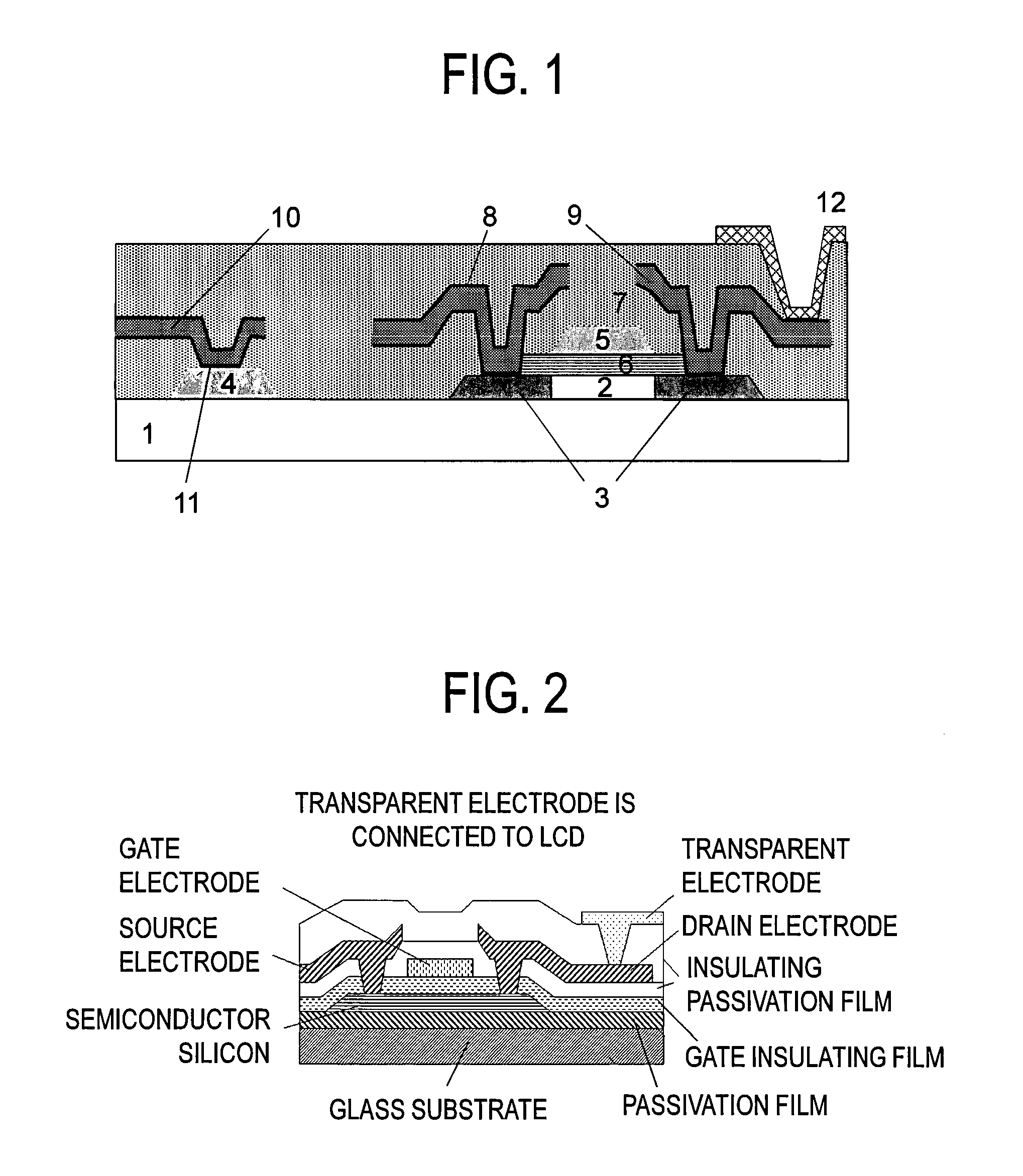
As just described the scan line 4 could be subjected to high temperature of about 450° C. to 600° C. The Al-based alloys for use in wiring of TFTs disclosed in the patent literatures 1-5 are, however, insufficient in terms of heat resistance at high temperatures.
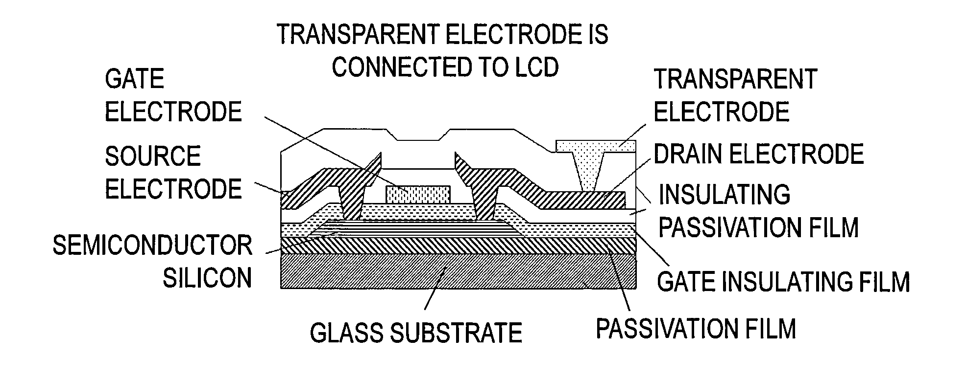
Due to poor resistance to hydrofluoric acid, conventional Al-based alloy thin films had a problem of dissolving by cleaning using hydrofluoric acid solution of polycrystalline silicon layer 3 and via hole 11 in the TFT structure illustrated in FIG. 1.

Method used


Image

  • Wiring structure for display device
  • Wiring structure for display device
  • Wiring structure for display device

Examples


example 1

[0130]In this example, samples of the first wiring structure were prepared as shown in Table 1. Each nitride film of various compositions shown in Table 1 was deposited as the second layer on Al alloys of compositions shown in the same table (the first layer). After the heat treatment at 450° C. to 600° C., electrical resistance, heat resistance (hillock density), and resistance to hydrofluoric acid of the wiring structures were evaluated. All of the Al alloys of the first layer used for this example are Al-group X element-REM alloys which satisfy the requirements of the present invention. In the tables, atomic percent is described as at %.

[0131]Firstly, the Al-0.5 at % Ta-2.0 at % Nd-0.1 at % Ni-0.5 at % Ge, Al-0.5 at % Ta-2.0 at % Nd-0.1 at % Ni-0.5 at % Ge-0.35 at % Zr, or Al-0.5 at % Ta-2.0 at % La-0.1 at % Ni-0.5 at % Ge alloy films (the first layer with a thickness of 300 nm) were deposited by a DC magnetron sputtering method on glass substrate (Eagle-XG, manufactured by Corni...

example 2

[0145]In this example, the wiring structure was prepared in the same manner as for Example 1 except that Al alloy for the first layer and nitride for the second layer were varied as shown in Tables 2-5. After the heat treatment at 450° C. to 600° C., electrical resistance, heat resistance (hillock density), and resistance to hydrofluoric acid of the wiring structures were evaluated in the same manner as Example 1.

[0146]The results are shown in Tables 2-5.

TABLE 2AThe second layerHeat Resistance (thickness: The first layerresistanceto50 nm)(thickness: 300 nm)Wiring resistance(hillock density)0.5% HFNo.CompositionComposition450° C.550° C.600° C.600° C.600° C.1Ti—NAl-0.1 at % Ta-0.3 at % Nd-0.1 at % Ni-0.5 at % Geexcellentexcellentexcellentexcellentexcellent2Ti—NAl-0.1 at % Ta-0.3 at % La-0.1 at % Ni-0.5 at % Geexcellentexcellentexcellentexcellentexcellent3Ti—NAl-0.1 at % Ta-0.6 at % Nd-0.1 at % Ni-0.5 at % Geexcellentexcellentexcellentexcellentexcellent4Ti—NAl-0.1 at % Ta-0.6 at % La-0...

example 3

[0149]In this example, as the second wiring structure, each of the second and third layers of various compositions was deposited in that order on each of the Al alloy (the first layer) shown in Table 6. After the heat treatment at 450° C. to 600° C., electrical resistance, heat resistance (hillock density), and resistance to hydrofluoric acid of the wiring structures were evaluated in the same manner as Example 1. All of the Al alloys of the first layer adopted in this example are Al-group X element-REM alloys which satisfy the requirements of the present invention.

[0150]Specifically, each of Al alloy film of Table 6 (the first layer, thickness: 300 nm) was first deposited on a glass substrate in the same manner as described in Example 1.

[0151]Next, each of nitride film No. 1-50 of Table 6 (the second layer, thickness: 50 nm) was deposited in the same manner as described in Example 1.

[0152]Each of the No. 1-50 metal films (the third layer with a thickness of 20 nm) described in Tabl...


PUM

PropertyMeasurementUnit
thicknessaaaaaaaaaa
thicknessaaaaaaaaaa
sizeaaaaaaaaaa

Abstract

Provided is a wiring structure for display device which does not generate hillocks even when exposed to high temperatures at levels around 450 to 600° C., has excellent high-temperature heat resistance, keeps electrical resistance (wiring resistance) of the entire wiring structure low, and further has excellent resistance to hydrofluoric acid. This wiring structure for a display device comprises a structure in which are laminated, in order from the substrate side, a first layer of an Al alloy that contains at least one chemical element selected from the group (group X) consisting of Ta, Nb, Re, Zr, W, Mo, V, Hf, Ti, Cr, and Pt and contains at least one rare earth element, and a second layer of an Al alloy nitride, or a nitride of at least one chemical element selected from the group Y consisted of Ti, Mo, Al, Ta, Nb, Re, Zr, W, V, Hf, and Cr.

Description

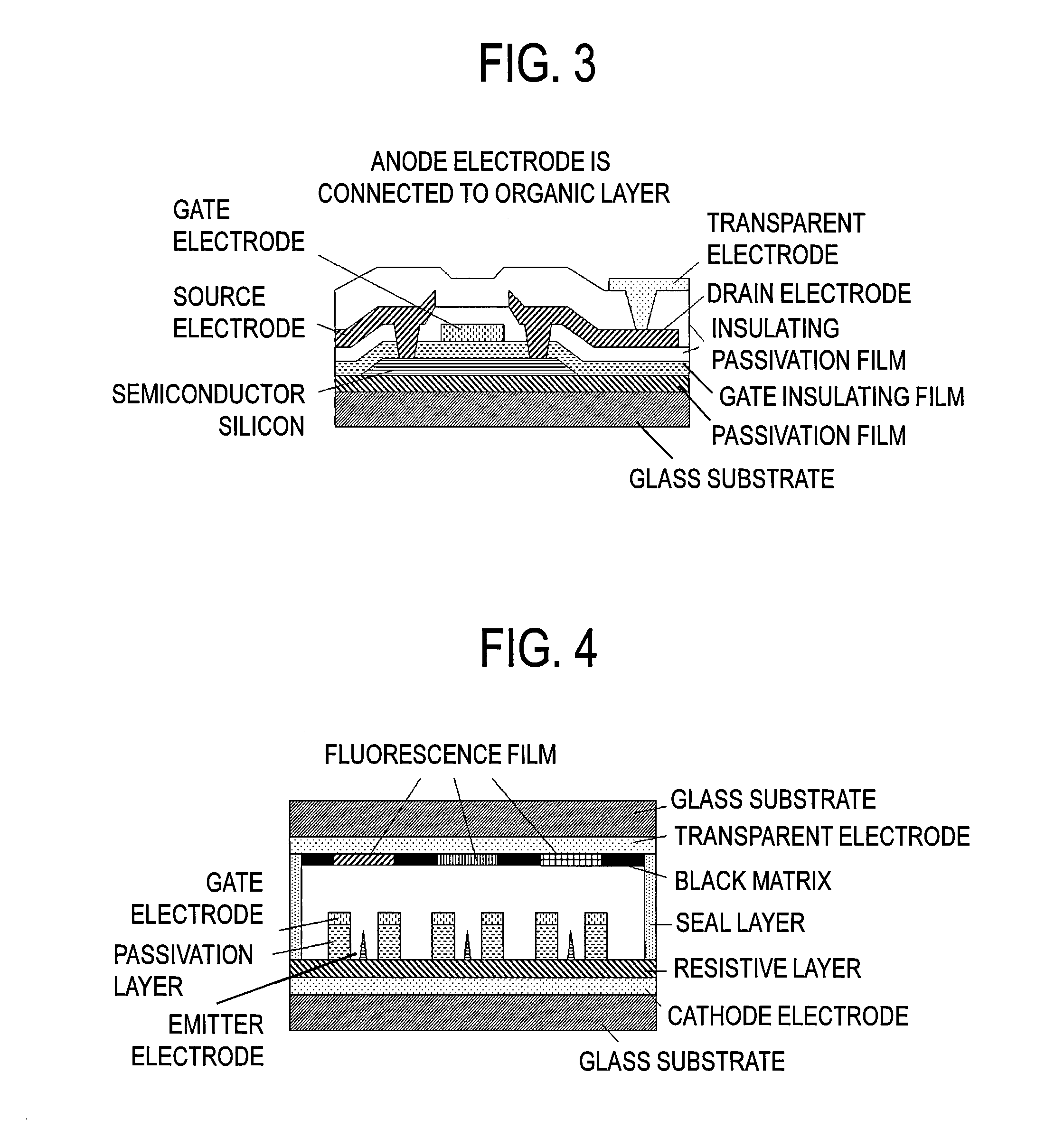
TECHNICAL FIELD[0001]The present invention relates to a wiring structure having an Al alloy film and being useful as an electrode and a wiring material for use in a display device such as a liquid crystal display, a fabrication method of the wiring structure, a display device comprising the wiring structure.BACKGROUND ART[0002]Aluminum alloy films for use in display devices are mainly used as electrodes and wiring materials. Examples of the electrodes and wiring materials include gate, source, and drain electrodes for a thin film transistor and a wiring material in a liquid crystal display (LCD); gate, source, and drain electrodes for a thin film transistor and a wiring material in an organic EL (OLED); cathode and gate electrodes and a wiring material in a field emission display (FED); an anode electrode and a wiring material in a vacuum fluorescent display (VFD); an address electrode and a wiring material in a plasma display panel (PDP); and a back electrode in an inorganic EL.[00...

Claims


Application Information

Patent Timeline
Patent Type & Authority Applications(United States)
IPC IPC(8): H01L23/532H01L21/48G02F1/1343
CPCH01L23/53219H01L21/4885G02F1/13439H01L23/53223B32B15/016B32B15/017C22C21/00C23C14/0641H01J11/46H01J31/127H01L27/124H01L2924/0002G02F1/136286C23C14/0036C23C14/025C22C14/00C22C27/02C22C27/04Y10T428/265Y10T428/31678C09K2323/061C09K2323/00G02F1/136295H01L2924/00H01L21/28H01L21/3205
Inventor OKUNO, HIROYUKIKUGIMIYA, TOSHIHIRO
Owner KOBE STEEL LTD
Learn More