
Multimode interference coupler for use with slot photonic crystal waveguides

a multi-mode interference and coupler technology, applied in the field of optical waveguides, can solve the problems of increasing the cost and complexity of the coupler, the coupler does not permit the optical path of the planer waveguide to be longitudinally aligned with the optical path of the pcw, etc., and achieves the effects of compact structure, improved efficiency and practicality, and improved efficiency

Active Publication Date: 2012-05-29
BOARD OF RGT THE UNIV OF TEXAS SYST
View PDF27 Cites 14 Cited by
  • Summary
  • Abstract
  • Description
  • Claims
  • Application Information

AI Technical Summary

Benefits of technology

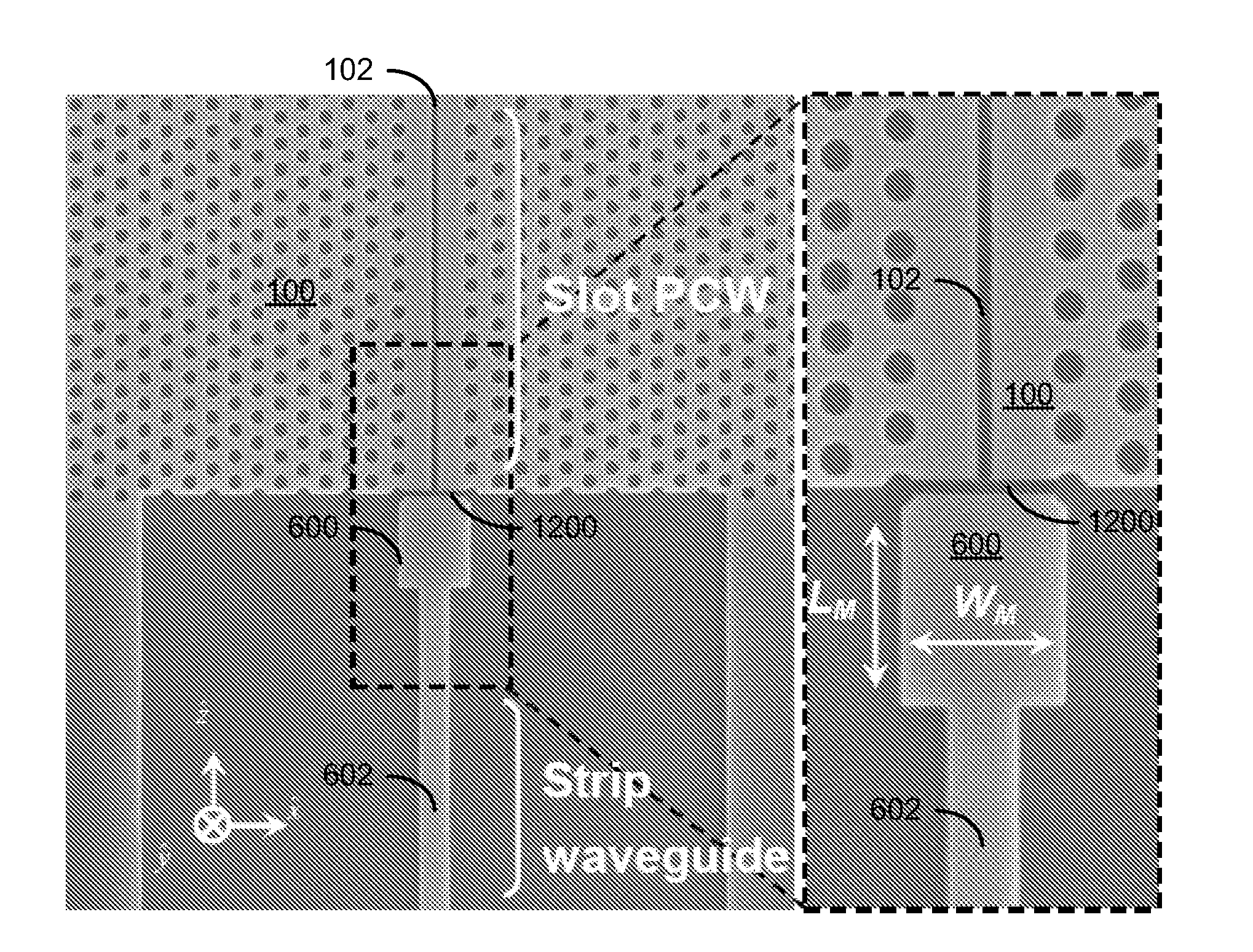
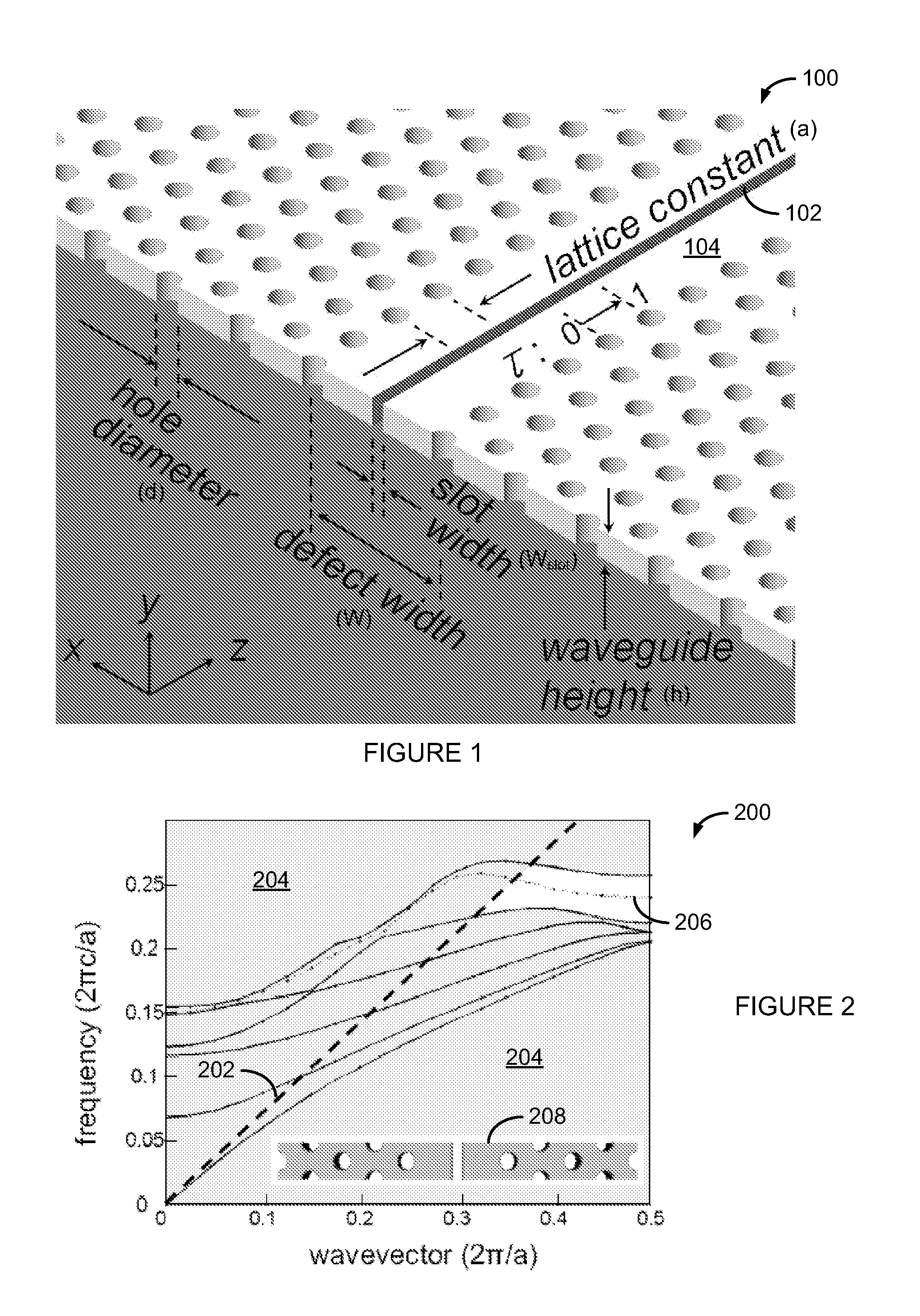
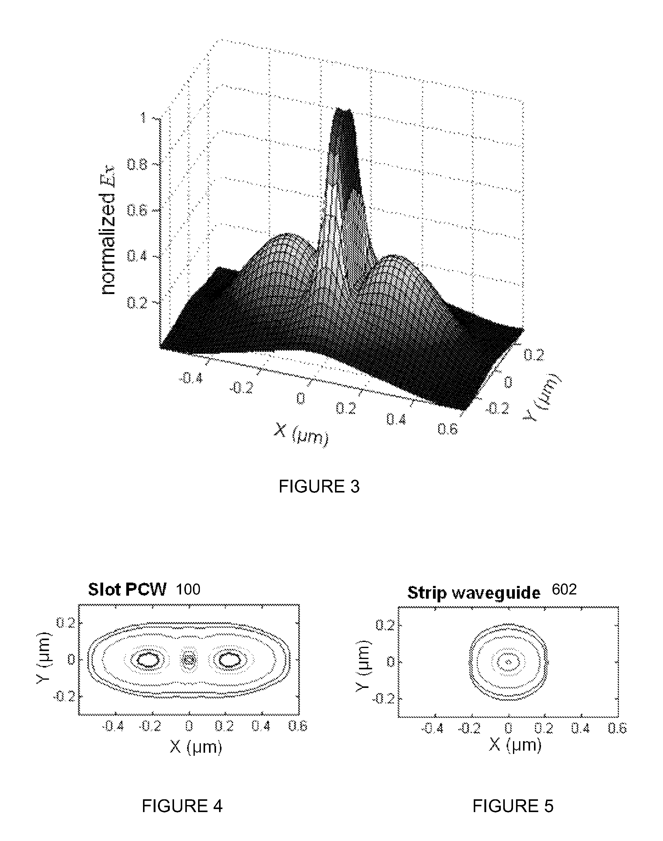
[0010]The present invention provides a novel multimode interference (MMI) coupler or structure integrated with a slot photonic crystal waveguide (PCW) for guiding light with low group velocity in a 100-nm-wide low-index region that provides unexpected results when: (a) the width (LM) of the MMI coupler is adjusted to set the phase difference close to π; and (b) the termination parameter (τ) is set to 0. The MMI coupler provides a 20 dB efficiency enhancement over a 35 nm optical bandwidth centered at the communication wavelength of 1550 nm compared with direct coupling configuration and has a coupling efficiency that exceeds 90%. In addition, the MMI coupler implements a more compact structure (e.g., 1.25 μm) compared to tapered MMI couplers (e.g., 10-500+ μm). As a result, the MMI coupler is a more efficient and practical device (cost, design, fabrication, reliability and power consumption) than prior art devices. These advantages are crucial for fully embedded board level interconnect where heat dissipation due to the fully embedded structure is a paramount concern. Moreover, the present invention can be used in sensors (e.g., bio-sensors, chemical sensors, structural sensors, etc.), telecommunications, fiber optics and data communications (e.g., routers, fully embedded board level interconnects, etc.) to name a few.
[0014]The present invention also provides a method for improving performance of an optical communication system by designing a multimode interference coupler having a width that is approximately equal to 1.6√{square root over (3α)} where α is a lattice constant of a slot photonic crystal waveguide, a length that is approximately equal to π / (β0−β2) where β0 is a fundamental mode propagation constant in the multimode interference coupler and β2 is a second order propagation constant in the multimode interference coupler. The multimode interference coupler is then fabricated between a strip waveguide and the slot photonic crystal waveguide such that the multimode interference coupler interfaces with the slot photonic crystal waveguide at an edge of a period that gives a termination parameter of approximately zero.
[0017]Note that the step of patterning the hexagonal lattice photonic crystal slab layer can further form an insulation gap disposed between the multimode interference coupler and the slot photonic crystal waveguide, wherein the length of the multimode interference coupler is reduced by approximately one half of a width of the insulation gap.

Problems solved by technology

Although the mirrored coupler provides a coupling efficiency of greater than 80%, the coupler does not permit the optical path of the planer waveguide to be longitudinally aligned with the optical path of the PCW.
In addition, the actual coupling efficiency of the coupler is dependant on the manufacturing quality of the mirror, which necessarily increases the cost and complexity of the coupler.

Method used


Image

  • Multimode interference coupler for use with slot photonic crystal waveguides
  • Multimode interference coupler for use with slot photonic crystal waveguides
  • Multimode interference coupler for use with slot photonic crystal waveguides

Examples


Embodiment Construction

[0042]While the making and using of various embodiments of the present invention are discussed in detail below, it should be appreciated that the present invention provides many applicable inventive concepts that can be embodied in a wide variety of specific contexts. The specific embodiments discussed herein are merely illustrative of specific ways to make and use the invention and do not delimit the scope of the invention.

[0043]To facilitate the understanding of this invention, a number of terms are defined below. Terms defined herein have meanings as commonly understood by a person of ordinary skill in the areas relevant to the present invention. Terms such as “a”, “an” and “the” are not intended to refer to only a singular entity, but include the general class of which a specific example may be used for illustration. The terminology herein is used to describe specific embodiments of the invention, but their usage does not delimit the invention, except as outlined in the claims.

[...


PUM

PropertyMeasurementUnit
lengthaaaaaaaaaa
lengthaaaaaaaaaa
lengthaaaaaaaaaa

Abstract

The present invention provides an optical apparatus having a multimode interference coupler configured to optically couple a strip waveguide to a slot photonic crystal waveguide. The multimode interference coupler has a coupling efficiency to the slot photonic crystal waveguide greater than or equal to 90%, a width that is approximately equal to a defect width of the slot photonic crystal waveguide, a length that is equal to or less than 1.5 μm, and interfaces with the slot photonic crystal waveguide at an edge of a period that gives a termination parameter of approximately zero. The optical apparatus may also include an insulation gap disposed between the multimode interference coupler and the slot photonic crystal waveguide, wherein the length of the multimode interference coupler is reduced by approximately one half of a width of the insulation gap.

Description

CROSS-REFERENCE TO RELATED APPLICATIONS[0001]This application claims benefit of U.S. provisional patent application Ser. No. 61 / 092,672 filed on Aug. 28, 2008 which is incorporated herein by reference in its entirety.STATEMENT OF FEDERALLY FUNDED RESEARCH[0002]This invention was made with U.S. Government support under contract number FA9550-05-C-0171 awarded by the Air Force Office of Scientific Research. The government has certain rights in this invention.TECHNICAL FIELD OF THE INVENTION[0003]The present invention relates in general to the field of optical waveguides, and more particularly to multimode interference couplers.BACKGROUND OF THE INVENTION[0004]Without limiting the scope of the invention, its background is described in connection with multimode interference couplers and photonic crystal waveguides. Introducing line defects into a photonic crystal lattice permits an electromagnetic wave having a frequency within the bandgap of the structure to be guided through the photo...

Claims


Application Information

Patent Timeline
Patent Type & Authority Patents(United States)
IPC IPC(8): G02B6/26H01L21/00G03F1/00
CPCB82Y20/00G02B6/1225G02B6/29344
Inventor CHEN, XIAONANCHEN, RAY T.
Owner BOARD OF RGT THE UNIV OF TEXAS SYST
Learn More