Memory cell array of memory

a memory and memory technology, applied in the field of memory, can solve the problem that the circuit layout area of the bit line transistor cannot be reduced, and achieve the effect of reducing the circuit layout area of the bit line transistor

Active Publication Date: 2012-06-12
MACRONIX INT CO LTD
View PDF4 Cites 0 Cited by
  • Summary
  • Abstract
  • Description
  • Claims
  • Application Information

AI Technical Summary

Benefits of technology

[0006]The invention is directed to a memory cell array of a memory, in which an array cell is used to replace a conventional MOS transistor so that a circuit layout area of bit line transistors (BLTs) may be reduced.

Problems solved by technology

However, the conventional bit line transistor is a metal-oxide semiconductor (MOS) transistor, so the circuit layout area of the of the bit line transistor cannot be reduced due to the limitations of the contact holes and the manufacturing processes of the MOS transistor.

Method used


Image

  • Memory cell array of memory
  • Memory cell array of memory
  • Memory cell array of memory

Examples


first embodiment

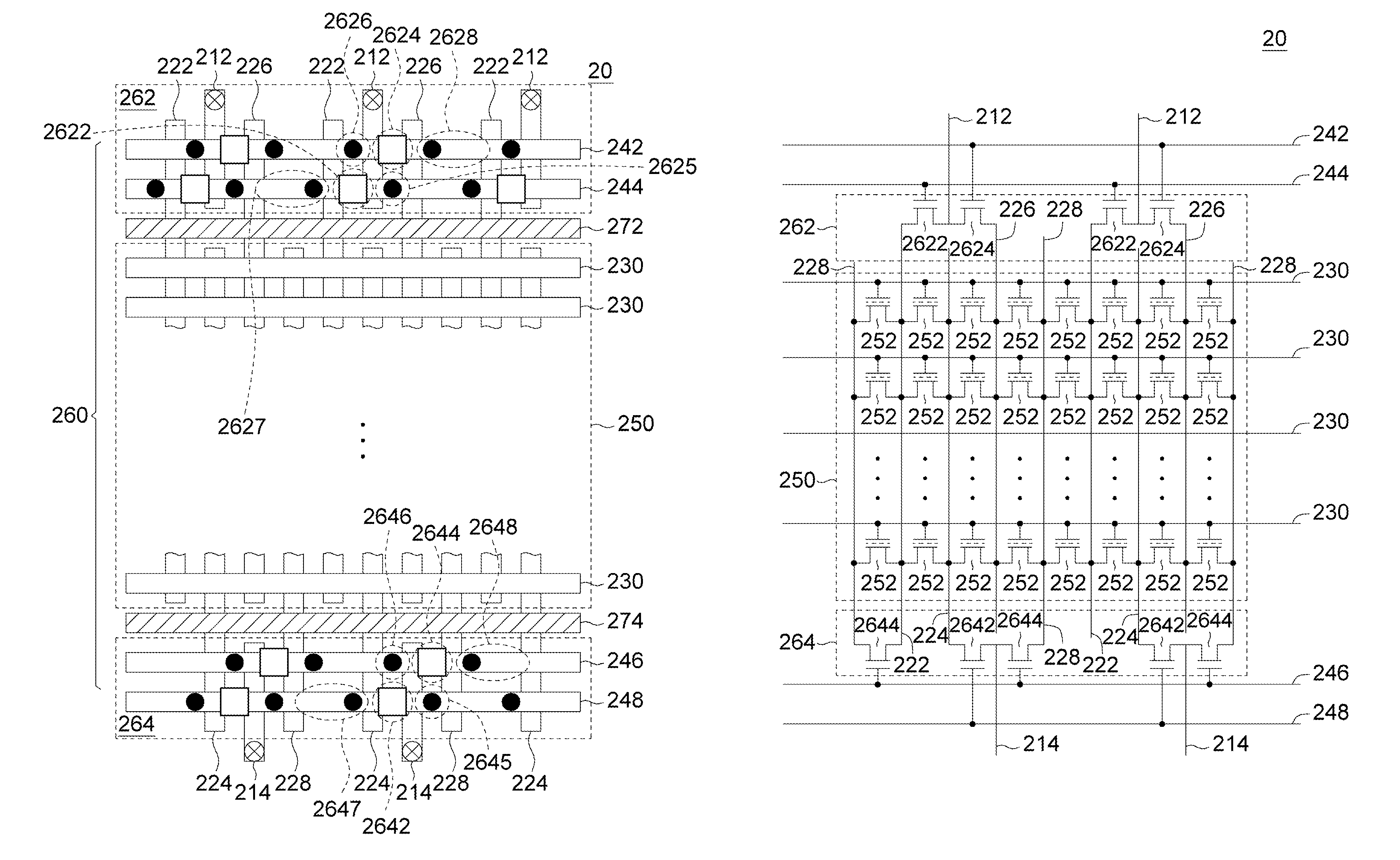
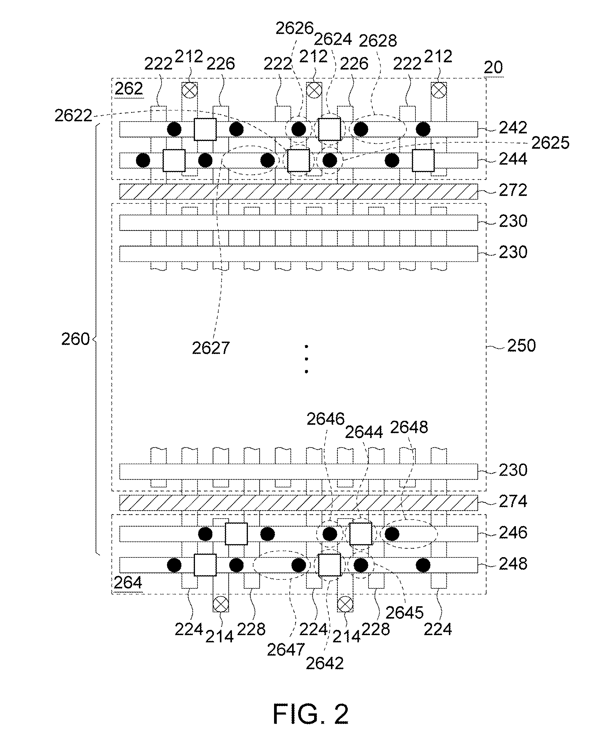
[0023]FIG. 2 is a schematic illustration showing a partial circuit layout of a memory cell array 20 of a memory according to a first embodiment of the invention. FIG. 3 is an equivalent circuit diagram showing a portion of the memory cell array of the memory according to the first embodiment of the invention. As shown in FIGS. 2 and 3, the memory cell array 20 of the memory is a virtual ground array memory, for example. The memory cell array 20 includes a main memory cell array 250 and a selected array 260. The main memory cell array 250 includes local bit lines 222, local bit lines 224, local bit lines 226, local bit lines 228, word lines 230 and memory cells. Each memory cell for storing data corresponds to and is connected to one of the local bit lines and one of the word lines.

[0024]The selected array 260 includes a bit line select unit 262 and a bit line select unit 264. The local bit lines 222 and the local bit lines 226 extend from the main memory cell array 250 to the bit li...

second embodiment

[0037]FIG. 4 is a schematic illustration showing a partial circuit layout of a memory cell array 30 of a memory according to a second embodiment of the invention. As shown in FIG. 4, the differences between the memory cell array 30 and the memory 20 will be described in the following. The memory cell array 30 further includes a backup selected array 360. The backup selected array 360 includes a backup bit line select unit 362 and a backup bit line select unit 364. When the bit line select unit 262 fails, the backup bit line select unit 362 is adopted to replace the failed bit line select unit 262. Similarly, when the bit line select unit 264 fails, the backup bit line select unit 364 is adopted to replace the failed bit line select unit 264.

[0038]The backup bit line select unit 362 includes a global bit line 312, a BLT control line 242, a BLT control line 244, a transistor 3622, a transistor 3624 and fixed value memory cells 3625 and 3627. Each of the transistor 3622, the fixed valu...

third embodiment

[0042]FIG. 5 is a schematic illustration showing a partial circuit layout of a memory cell array 40 according to a third embodiment of the invention. FIG. 6 is an equivalent circuit diagram showing a portion of the memory cell array according to the third embodiment of the invention. As shown in FIGS. 5 and 6, the difference between the memory cell array 40 and the memory cell array 20 resides in that the select unit 460 is different from the select unit 260. The select unit 460 includes a bit line select unit 462 and a bit line select unit 464. The local bit line 222 and the local bit line 226 extend from the main memory cell array 250 to the bit line select unit 462, while the local bit line 224 and the local bit line 228 extend from the main memory cell array 250 to the bit line select unit 464.

[0043]In addition to the BLT control line 242, the BLT control line 244, the transistor 2622, the transistor 2624 and the fixed value memory cells 2625 to 2628, the bit line select unit 46...


PUM


Abstract

A memory cell array of a memory comprises a main memory cell array, including local bit lines, word lines and memory cells, and a selected array, including a global bit line, a bit line transistor (BLT) control line, a transistor and a fixed value memory cell. The local bit lines comprise first and second local bit lines. Each memory cell for storing data corresponds and is connected to one local bit line and one word line. The transistor is coupled to the global bit line, first local bit line and BLT control line, and selectively turns on to connect the global bit line to the first local bit line. The fixed value memory cell coupled to the global bit line, second local bit line, and BLT control line is programmed to a fixed value so that a threshold voltage thereof is greater than a threshold voltage of the transistor.

Description

BACKGROUND OF THE INVENTION[0001]1. Field of the Invention[0002]The invention relates in general to a memory, and more particularly to a memory cell of a memory using array cells to form bit line transistors (BLTs).[0003]2. Description of the Related Art[0004]FIG. 1 (Prior Art) is an equivalent circuit diagram showing a portion of a memory cell array 10. Referring to FIG. 1, the memory cell array 10 includes a memory cell 150, bit line transistors (BLTs) 131 to 138, BLT control lines 141 to 148, word lines 161 and 162, a global word line 112, a global word line 114, a global word line 116, a global word line 118 and local bit lines 121 to 128. The bit line transistors 131 to 138 control to select which local bit line for the programming operation, and the bit line transistors 131 to 138 are respectively controlled by the BLT control lines 141 to 148.[0005]However, the conventional bit line transistor is a metal-oxide semiconductor (MOS) transistor, so the circuit layout area of the ...

Claims


Application Information

Patent Timeline
Patent Type & Authority Patents(United States)
IPC IPC(8): G11C11/34
CPCG11C16/0483G11C16/30G11C16/10
Inventor CHEN, CHUNG-KUANG
Owner MACRONIX INT CO LTD
Why Eureka
Try Eureka