Structure having silicon CMOS transistors with column III-V transistors on a common substrate

a technology of silicon cmos transistors and silicon cmos transistors, applied in the field of semiconductor structures, can solve the problems of increasing the footprint, limiting the integration complexity, and expensive processes

Active Publication Date: 2012-07-03
RAYTHEON CO
View PDF10 Cites 34 Cited by
  • Summary
  • Abstract
  • Description
  • Claims
  • Application Information

AI Technical Summary

Benefits of technology

[0002]As is known in the art, many electronics applications incorporate both silicon and column III-V circuits due to their unique performance characteristics. The silicon circuits are typically CMOS circuits used for digital signals and the column III-V circuits are for microwave, millimeterwave, and optical signals. Typically this integration is done by fabricating the silicon and column III-V circuits separately on different chips and then electrically connecting them, often with wire bonds. This process is expensive, limits integration complexity, increases the footprint, and introduces parasitic resistances and inductances which degrade circuit performance.
[0005]It is also known that it is desirable to have silicon CMOS transistors and column III-V (e.g. GaN, GaAs or InP) transistors on a common substrate. One structure used to form CMOS transistors and column III-V transistors on a common substrate is shown in FIG. 1. There, a GaAs transistor is formed on the same substrate as the CMOS transistors. It is also known that GaAs grown on a growth layer having a <100> crystallographic orientation provides a layer with a minimum number of crystalline defects. To provide this <100> growth layer for the GaAs device, a Ge layer having a <100> crystallographic orientation is used, as shown in FIG. 1 of the disclosure. However, Ge melts at 938 degrees C. and thereby limits the fabrication temperatures used in fabricating the CMOS devices. Also, Ge causes cross doping of the GaAs device resulting in increased microwave power loss. Additionally the starting wafer in FIG. 1 requires two layer transfers which is an expensive process.
[0007]The inventors have recognized that there is an advantage in modifying the SOI structure described above by using a silicon substrate having a <111> crystallographic orientation rather than a <100> crystallographic orientation so that the column III-N device can be formed on the same <111> crystallographic orientation substrate as the CMOS devices with such substrate being crystallographically matched to the preferred <111> crystallographic orientation for the column III-N device. An additional advantage recognized by the inventors is having both the <111> silicon orientation and the <100> silicon orientation present in the starting wafer so that column III-As, column III-P and column III-Sb devices, which grow with fewest defects on the <100> orientation, can also be combined on the same substrate with column III-N devices and CMOS.

Problems solved by technology

This process is expensive, limits integration complexity, increases the footprint, and introduces parasitic resistances and inductances which degrade circuit performance.
Many years ago, CMOS was formed on silicon substrates having crystallographic orientations; however this orientation is inferior for CMOS than the crystallographic orientation due to a higher surface state density on crystallographic orientation.
However, Ge melts at 938 degrees C. and thereby limits the fabrication temperatures used in fabricating the CMOS devices.
Also, Ge causes cross doping of the GaAs device resulting in increased microwave power loss.
Additionally the starting wafer in FIG. 1 requires two layer transfers which is an expensive process.

Method used


Image

  • Structure having silicon CMOS transistors with column III-V transistors on a common substrate
  • Structure having silicon CMOS transistors with column III-V transistors on a common substrate
  • Structure having silicon CMOS transistors with column III-V transistors on a common substrate

Examples


Embodiment Construction

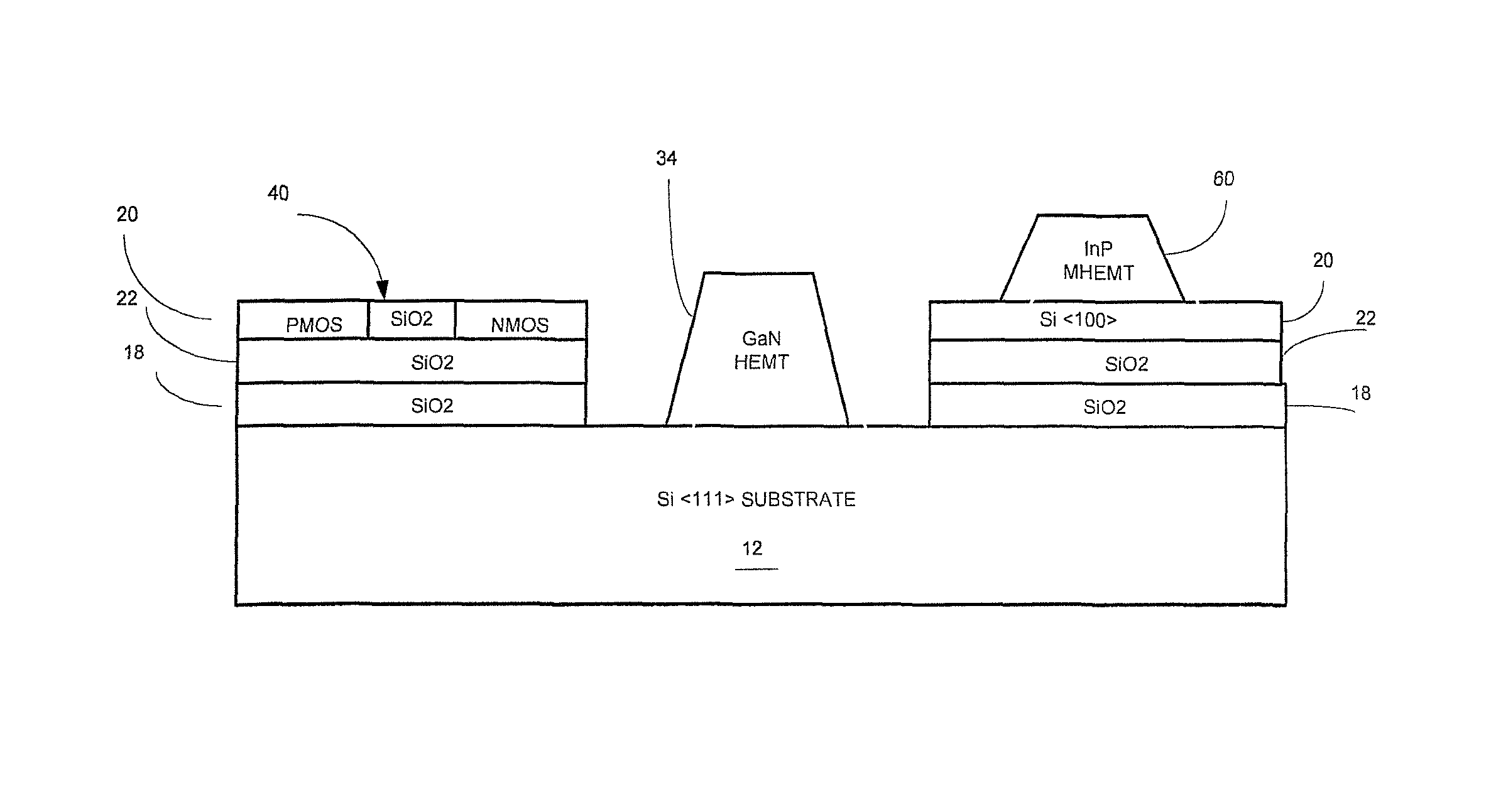
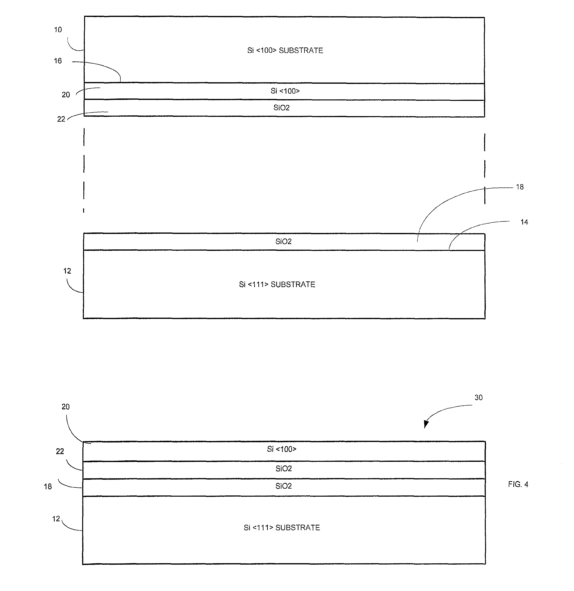
[0027]Referring now to FIG. 3, a pair of silicon wafers 10, 12 or substrates are shown in an exploded view. One of the substrates 12 has a crystallographic orientation (i.e., the crystallographic axis is normal to the upper surface 14 of the substrate) and the other one of the substrates 10 has a crystallographic orientation (i.e., the crystallographic axis is normal to the 16 surface of the substrate). The substrate 12 has a layer 18 of silicon dioxide formed thereof by any conventional technique.

[0028]The other substrate 10 has a silicon layer 20, in the order of several microns, of silicon with a crystallographic orientation formed on surface 16 of the substrate 10 thereof by any convention techniques such as for example epitaxial growth. The active layer 20 is doped in any conventional manner for the desired CMOS application. A layer 22 of silicon dioxide is formed by conventional deposition or growth on the silicon layer 20. The surfaces of silicon dioxide layers 18, 22 ar...


PUM


Abstract

A semiconductor structure having: a silicon substrate having a crystallographic orientation; an insulating layer disposed over the silicon substrate; a silicon layer having a different crystallographic orientation than the crystallographic orientation of the substrate disposed over the insulating layer; and a column III-V transistor device having the same crystallographic orientation as the substrate disposed on the silicon substrate. In one embodiment, the column III-V transistor device is in contact with the substrate. In one embodiment, the device is a GaN device. In one embodiment, the crystallographic orientation of the substrate is <111> and wherein the crystallographic orientation of the silicon layer is <100>. In one embodiment, CMOS transistors are disposed in the silicon layer. In one embodiment, the column III-V transistor device is a column III-N device. In one embodiment, a column III-As, III-P, or III-Sb device is disposed on the top of the <100> silicon layer.

Description

TECHNICAL FIELD[0001]This disclosure relates generally to semiconductor structures and more particularly to semiconductor structures having silicon CMOS transistors with column III-V transistors on a common substrate.BACKGROUND AND SUMMARY[0002]As is known in the art, many electronics applications incorporate both silicon and column III-V circuits due to their unique performance characteristics. The silicon circuits are typically CMOS circuits used for digital signals and the column III-V circuits are for microwave, millimeterwave, and optical signals. Typically this integration is done by fabricating the silicon and column III-V circuits separately on different chips and then electrically connecting them, often with wire bonds. This process is expensive, limits integration complexity, increases the footprint, and introduces parasitic resistances and inductances which degrade circuit performance.[0003]It is also known in the art that transistors have been formed on silicon having &l...

Claims


Application Information

Patent Timeline
Patent Type & Authority Patents(United States)
IPC IPC(8): H01L27/085
CPCH01L21/76251H01L21/8258H01L29/267H01L29/045H01L27/1207H01L29/04
Inventor HOKE, WILLIAM E.LAROCHE, JEFFREY R.
Owner RAYTHEON CO
Why Eureka
Try Eureka