Semiconductor device and method for forming the same

a semiconductor device and semiconductor technology, applied in the field of semiconductor devices and forming methods, can solve problems such as difficulty in reducing the entire area, and achieve the effect of preventing the deterioration of the properties of the semiconductor devi

Active Publication Date: 2012-07-10
SK HYNIX INC
View PDF7 Cites 0 Cited by
  • Summary
  • Abstract
  • Description
  • Claims
  • Application Information

AI Technical Summary

Benefits of technology

[0016]The present invention prevents the generation of a void when forming a buried gate electrode by making a width of a trench 2.5 to 3 times wider, and prevents deterioration of properties of a semiconductor device due to a void that is generated when forming buried gates by separating buried gate electrodes from each other through self-aligned dry etch.

Problems solved by technology

In the case of a complicated semiconductor memory device, it is difficult to reduce the entire area because the memory device includes a plurality of transistors.

Method used


Image

  • Semiconductor device and method for forming the same
  • Semiconductor device and method for forming the same
  • Semiconductor device and method for forming the same

Examples


Embodiment Construction

[0019]Hereinafter, the present invention is illustrated in detail according to an embodiment of the present invention with reference to attached drawings.

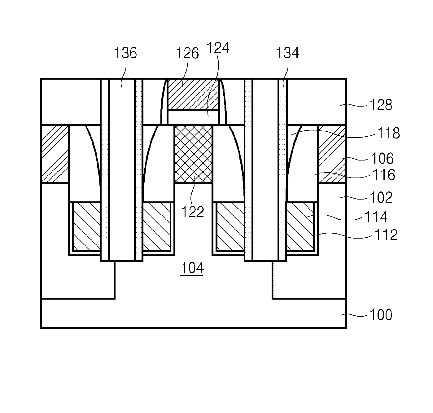
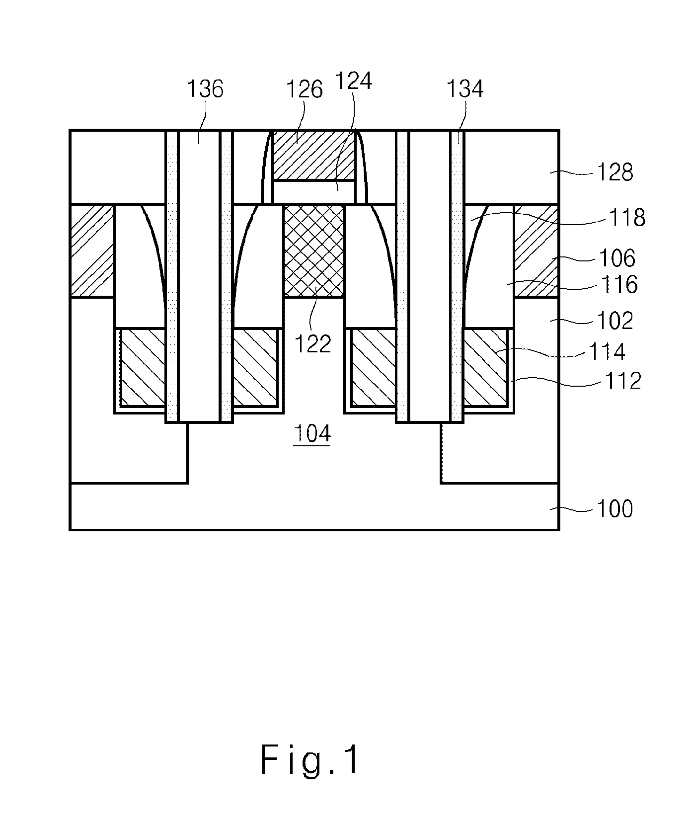
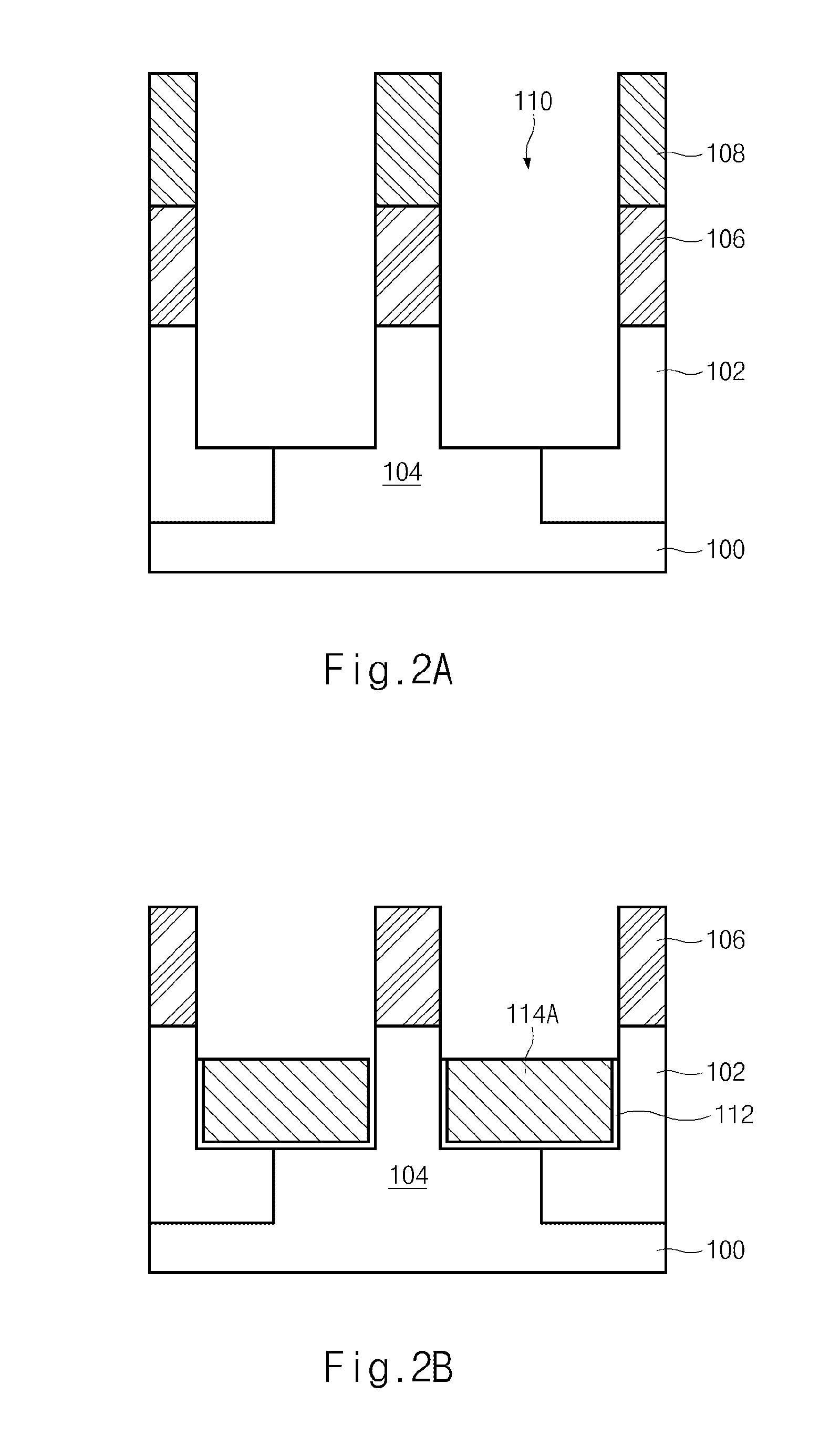
[0020]FIG. 1 is a cross-sectional view of a semiconductor device according to an embodiment of the present invention. FIGS. 2A to 2H are cross-sectional views showing a method of forming the semiconductor device

[0021]Referring to FIGS. 1 and 2A to 2H, the semiconductor device includes a buried gate including a passivation (or protection) layer pattern 116 and a gate electrode 114 formed on both sides of a trench 110 that is formed within a semiconductor substrate 100. The semiconductor substrate 100 includes an active region 104 defined by an device isolation region 102, and a storage node contact 136, which is buried between the buried gates, connected to the active region 104 and the device isolation region 102 in a middle portion of the trench 110. The semiconductor device further includes a spacer 134 formed on a sidewall of th...


PUM


Abstract

A semiconductor device includes a semiconductor substrate including an active area defined by an device isolation region, a buried gate formed on both side walls of a trench formed in the semiconductor substrate, and a storage node contact which is buried between the buried gates, and is connected to the active region of a middle portion of the trench and the device isolation region.

Description

CROSS-REFERENCES TO RELATED APPLICATIONS[0001]The present application claims priority to Korean patent application number 10-2009-0127900, filed on Dec. 21, 2009, which is incorporated by reference in its entirety.BACKGROUND OF THE INVENTION[0002]The present invention relates to a semiconductor device and a method of forming the semiconductor device, and more particularly, to a semiconductor device capable of substantially preventing the generation of a void when forming a buried gate electrode.[0003]Among semiconductor memory devices, a dynamic random access memory (DRAM) includes a plurality of unit cells each of which consists of a capacitor and a transistor. Here, the capacitor is used to temporarily store data, and the transistor is used to transmit data between a bit line and the capacitor in response to a control signal supplied through a word line. The transistor consists of three regions which are a gate, a source and a drain. Electric charges move between the source and th...

Claims


Application Information

Patent Timeline
Patent Type & Authority Patents(United States)
IPC IPC(8): H01L23/48
CPCH01L21/76897H01L27/10855H01L27/10876H01L27/10891H10B12/0335H10B12/053H10B12/488H01L21/2255H01L29/66348H01L29/7813
Inventor CHO, YOUNG MAN
Owner SK HYNIX INC
Why Eureka
Try Eureka