Multilayer wiring, semiconductor device, substrate for display device, and display device

a multi-layer wiring and display device technology, applied in non-linear optics, instruments, optics, etc., can solve problems such as power consumption and property deterioration, and achieve the effect of preventing property deterioration and reducing the area of the wiring layer

Active Publication Date: 2013-05-21
SHARP KK
View PDF9 Cites 1 Cited by
  • Summary
  • Abstract
  • Description
  • Claims
  • Application Information

AI Technical Summary

Benefits of technology

[0037]According to the present invention, it is possible to provide a multilayer wiring capable of reducing the area of the wiring layer while preventing the property deterioration due to the parasitic capacitance, a semiconductor device, a substrate for display device and a display device.

Problems solved by technology

This may cause property deterioration due to the parasitic capacitance such as signal delay in the wiring, inappropriate signal voltage, and increase in power consumption, which have to be improved.

Method used


Image

  • Multilayer wiring, semiconductor device, substrate for display device, and display device
  • Multilayer wiring, semiconductor device, substrate for display device, and display device
  • Multilayer wiring, semiconductor device, substrate for display device, and display device

Examples


embodiment 1

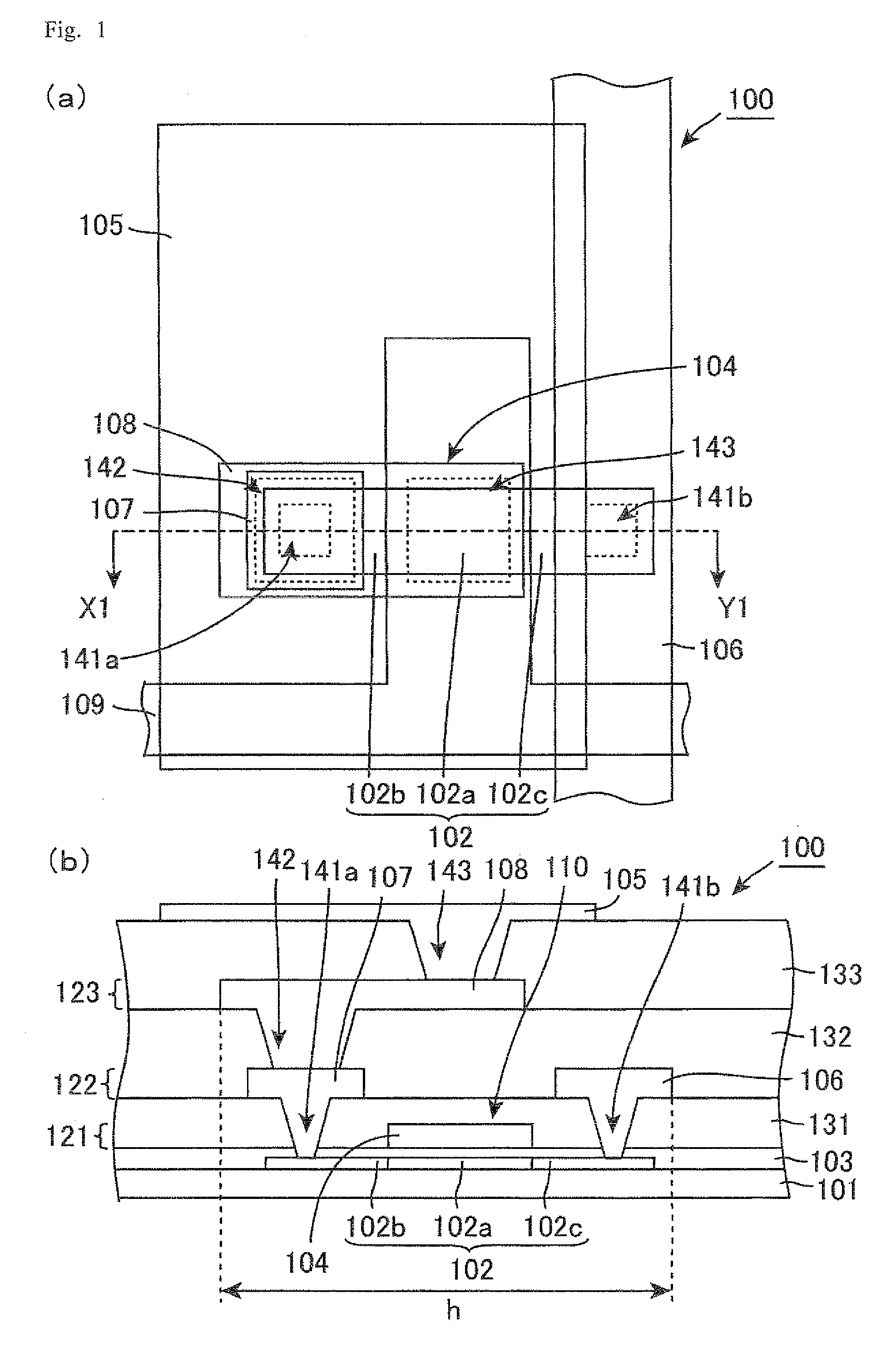
[0039]FIG. 1 are schematic views each illustrating a substrate for display device of Embodiment 1. FIG. 1(a) is a plan view of the substrate and FIG. 1(b) is a cross-sectional view of the substrate taken along X1-Y1 line in FIG. 1(a).

[0040]A substrate 100 for display device of Embodiment 1 is to be used in a display device such as a liquid crystal display device. As illustrated in FIGS. 1(a) and 1(b), the substrate 100 for display device comprises a semiconductor layer 102, a gate insulating layer 103, a wiring layer 121, an interlayer insulating layer 131, a wiring layer 122, an interlayer insulating layer 132, a wiring layer 123, an interlayer insulating layer 133, and a pixel electrode 105 laminated in this order on a main face of a substrate 101. The semiconductor layer 102 is a first conductor layer laminated on the substrate 101, and comprises a channel region 102a and high-concentration impurity regions 102b, 102c. The gate insulating layer 103 is a first insulating layer lam...

embodiment 2

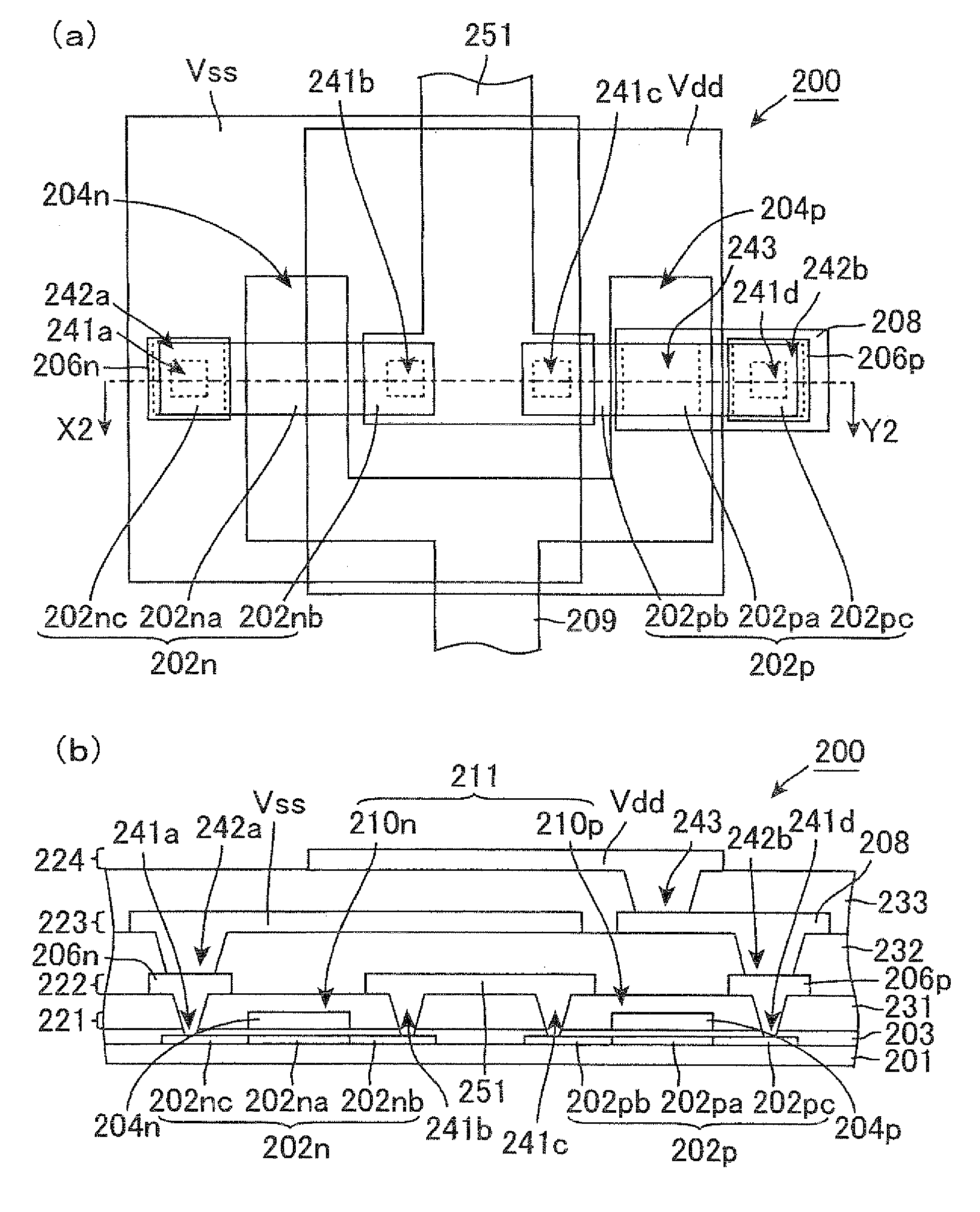
[0069]FIG. 5 are schematic views each illustrating a substrate for display device of Embodiment 2. FIG. 5(a) is a plan view of the substrate and FIG. 5(b) is a cross-sectional view of the substrate taken along X2-Y2 line in FIG. 5(a).

[0070]A substrate 200 for display device of Embodiment 2 is a substrate for display device to be used in a display device such as a liquid crystal display device. As illustrated in FIGS. 5(a) and 5(b), the substrate 200 for display device comprises a semiconductor layers 202n and 202p, a gate insulating layer 203, a wiring layer 221, an interlayer insulating layer 231, an interlayer insulating layer 232, a wiring layer 223, an interlayer insulating layer 233, and a wiring layer 224 laminated in this order on a main face of the substrate 201.

[0071]The semiconductor layers 202n and 202p are the first conductive layers laminated on the substrate 201. The gate insulating layer 203 is the first insulating layer laminated on the substrate 201. The wiring laye...


PUM


Abstract

The present invention provides a multilayer wiring capable of reducing the area of the wiring layer while preventing the property deterioration due to the parasitic capacitance, a semiconductor device, a substrate for display device, and a display device. The multilayer wiring of the present invention includes: a first conductor; a second conductor; and a third conductor. The first conductor is positioned in a (n+1)th conductive layer. The second conductor is positioned in a (n+2)th conductive layer, is electrically connected to a conductor in a layer below the (n+1)th conductive layer through at least a first connection hole in a (n+1)th insulating layer directly below the (n+2)th conductive layer, and is positioned so as not to overlap with the first conductor in a plan view of the main face of the substrate. The third conductor is positioned in a (n+3)th conductive layer, is electrically connected to a second conductor through a second connection hole in a (n+2)th insulating layer directly below the (n+3)th conductive layer, and is positioned on the second connection hole toward the first conductor. The second connection hole overlaps with the first connection hole in a plan view of the main face of the substrate.

Description

[0001]This application is the U.S. national phase of International Application No. PCT / JP2008 / 072665 filed 12 Dec. 2008, which designated the U.S. and claims priority to JP Application No. 2008-116177 filed 25 Apr. 2008, the entire contents of each of which are hereby incorporated by reference.TECHNICAL FIELD[0002]The present invention relates to a multilayer wiring, a semiconductor device, a substrate for display device, and a display device. More specifically, the present invention relates to a multilayer wiring, a semiconductor device, a substrate for display device, and a display device, which are suitably used in mobile devices such as mobile phones.BACKGROUND ART[0003]Recently, downsizing and weight saving are further demanded with respect to mobile electronic devices, such as mobile phones and PDA, on which display devices including liquid crystal display devices and organic electroluminescence displays are mounted. Along with this trend, downsizing of a non-opening part in a...

Claims


Application Information

Patent Timeline
Patent Type & Authority Patents(United States)
IPC IPC(8): H01L23/48H01L23/52H01L29/40
CPCG02F1/136286H01L23/528H01L27/124H01L27/1248G02F2001/13606G02F2001/13629H01L2924/12044H01L2924/0002H01L2924/00G02F1/13606G02F1/13629
Inventor MORIWAKI, HIROYUKI
Owner SHARP KK
Why Eureka
Try Eureka