Logical-to-physical address translation for solid state disks

a logical-to-physical address and solid-state disk technology, applied in the field of flash memory storage devices, can solve the problems of not providing full address and data bus capability, not allowing random access to memory locations, and additional bytes of memory, and achieve the effect of reducing the number of erasures

Active Publication Date: 2012-07-10
AVAGO TECH INT SALES PTE LTD
View PDF75 Cites 59 Cited by
  • Summary
  • Abstract
  • Description
  • Claims
  • Application Information

AI Technical Summary

Problems solved by technology

However, the I / O interface of NAND flash memory does not provide full address and data bus capability and, thus, generally does not allow random access to memory locations.
As such, the additional bytes of memory are “hidden” from the user and are not available for storing user data.
Thus, typical flash memories perform inefficiently for enterprise applications since there are unused bytes in each page.
Thus, the direct page mapping scheme requires a large amount of RAM (on the order of 1-2 MB per GB of user storage) to store the translation table, which can become burdensome for higher capacity SSDs.
However, because block mapping does not have a page-level map, the flash media may be inefficiently utilized when the data access workload is non-sequential.
However, because the spare area is used to store page-level mapping information, less memory is available for error correction codes (ECC).
Further, the limited amount of memory available in the spare area precludes storing complicating mapping information.
Finally, reconstruction of the translation table at startup can be time-intensive.
This inefficiency would reduce the realized flash memory capacity because less current data could be stored.
Garbage collection routines impact performance of the flash memory system by utilizing processor resources and potentially delaying write operations to the flash media.
Therefore, over the operational life of an SSD, blocks of flash memory will fail and become unusable.

Method used


Image

  • Logical-to-physical address translation for solid state disks
  • Logical-to-physical address translation for solid state disks
  • Logical-to-physical address translation for solid state disks

Examples


Embodiment Construction

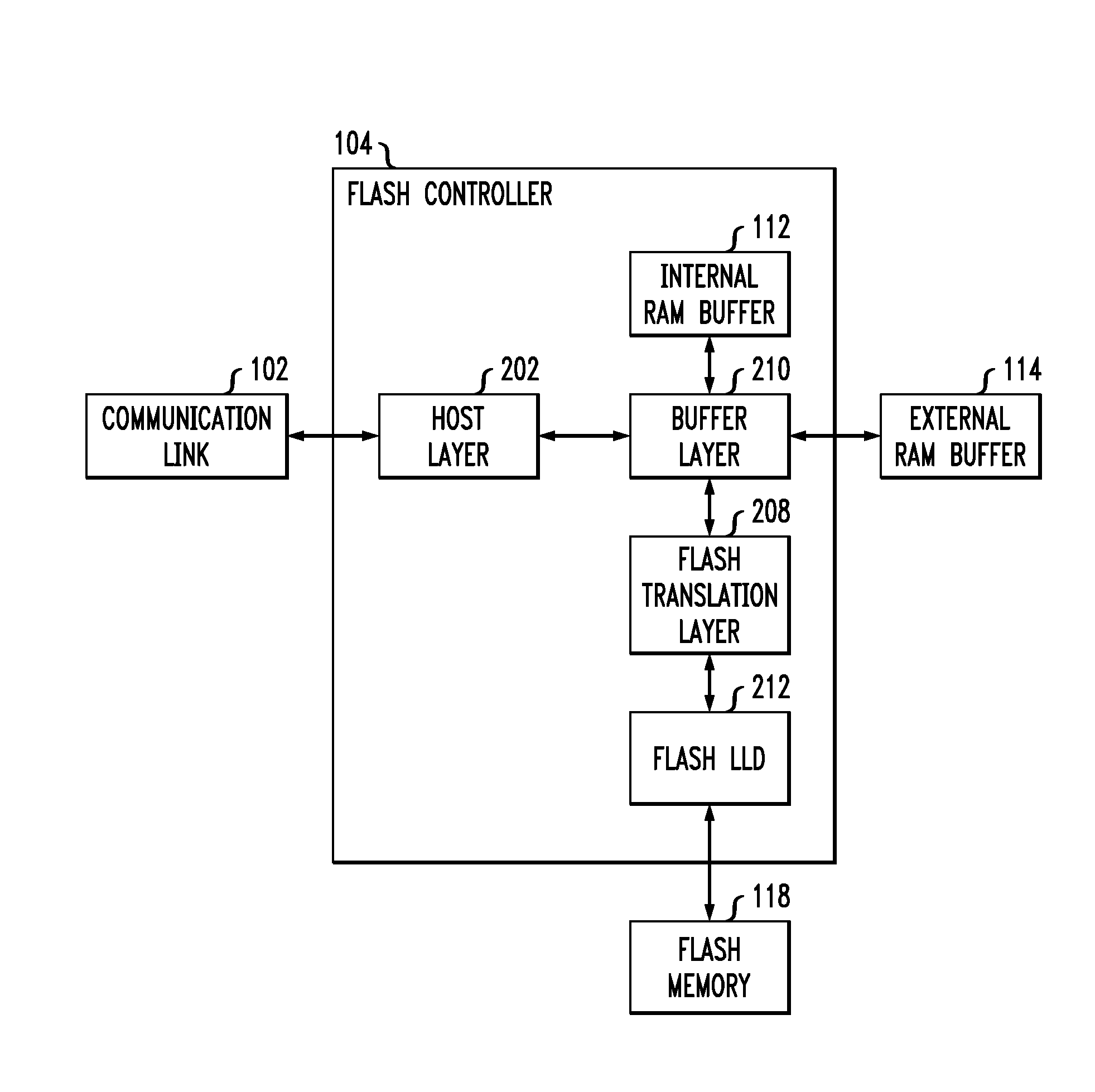
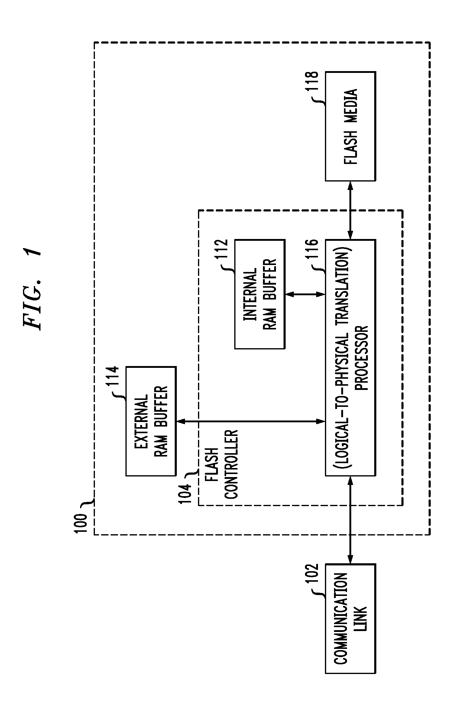
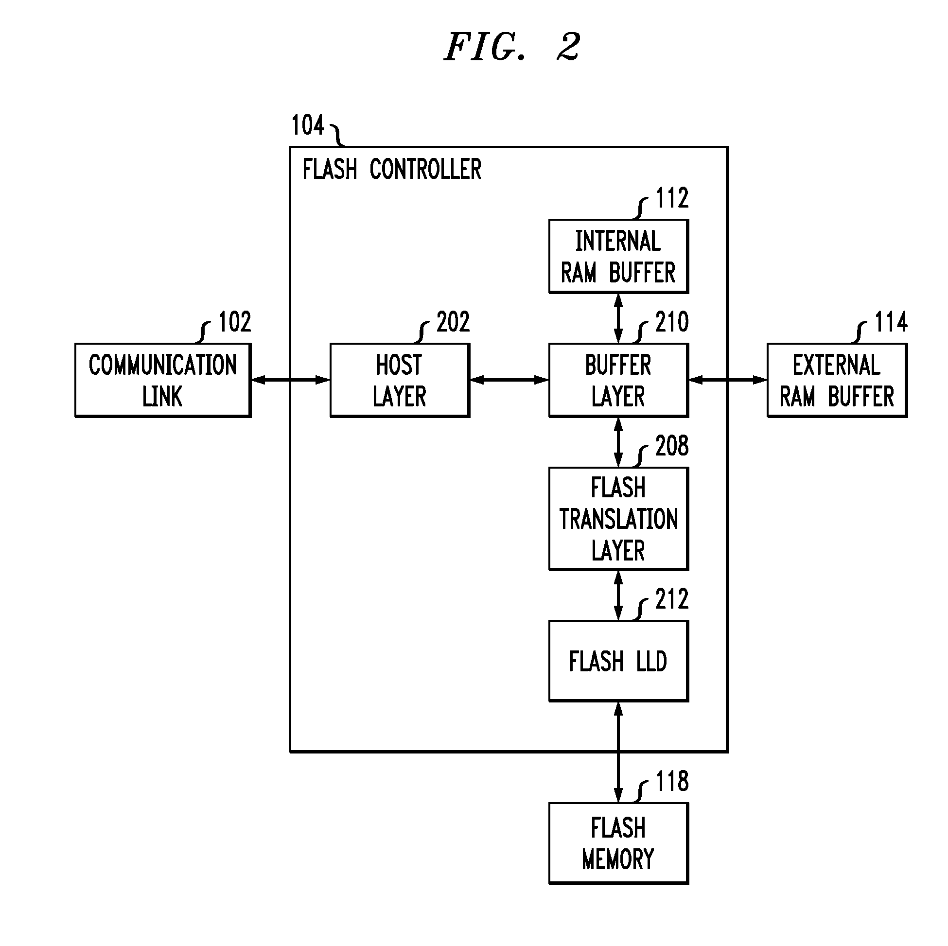
[0055]In accordance with embodiments of the present invention, a flash memory storage system is provided. The flash memory storage system employs logical-to-physical address translation to track when new data for a given logical block address (LBA) is written to an erased page that is a different physical page than the page previously used for that LBA. Embodiments of the present invention describe a flash memory storage system for use in Solid State Disk (SSD) applications, as well as in hybrid magnetic and solid state storage systems. In contrast to existing approaches in flash memory storage systems employing one of i) direct page mapping, ii) block mapping, and Superblock mapping for logical-to-physical address translation, embodiments of the present invention employ page level mapping with a superblock structure, allowing a logical page to be stored to any physical page within a superblock.

[0056]To provide efficient flash media write operations, an active block table might be e...


PUM


Abstract

Described embodiments provide logical-to-physical address translation for data stored on a storage device having sectors organized into blocks and superblocks. A flash translation layer maps a physical address in the storage device to a logical sector address. The logical sector address corresponds to mapping data that includes i) a page index, ii) a block index, and iii) a superblock number. The mapping data is stored in at least one summary page corresponding to the superblock containing the physical address. A block index and a page index of a next empty page in the superblock are stored in a page global directory corresponding to the superblock. A block index and a page index of the at least one summary page and the at least one active block table for each superblock are stored in at least one active block table of the storage device.

Description

CROSS-REFERENCE TO RELATED APPLICATIONS[0001]This application claims the benefit of the filing date of U.S. provisional application Nos. 61 / 245,112 filed Sep. 23, 2009, and 61 / 245,973 filed Sep. 25, 2009, the teachings of which are incorporated herein in their entireties by reference.[0002]The subject matter of this application is related to U.S. patent application Ser. Nos. 12 / 436,227 filed May 6, 2009, 12 / 475,710 filed Jun. 1, 2009, 12 / 475,716 filed Jun. 1, 2009, 12 / 477,996 filed Jun. 4, 2009, 12 / 478,013 filed Jun. 4, 2009, 12 / 508,879 filed Jul. 24, 2009, and 12 / 508,915 filed Jul. 24, 2009, the teachings of all of which are incorporated herein in their entireties by reference. The subject matter of this application is also related to U.S. patent application Ser. Nos. 12 / 643,471 filed Dec. 21, 2009, 12 / 649,490 filed Dec. 30, 2009, 12 / 722,828 filed Mar. 12, 2010, 12 / 730,627 filed Mar. 24, 2010, 12 / 731,631 filed Mar. 25, 2010, 12 / 767,985 filed Apr. 27, 2010, 12 / 768,058 filed Apr. 27,...

Claims


Application Information

Patent Timeline
Patent Type & Authority Patents(United States)
IPC IPC(8): G06F12/00
CPCG06F13/14G06F13/24G06F12/0246G06F12/1027G06F3/00G06F2212/7201G06F2213/0028G06F2212/7203
Inventor FORHAN, CARLHEMPSTEAD, PAMELAHICKEN, MICHAELREITER, RANDYSWATOSH, TIMOTHY
Owner AVAGO TECH INT SALES PTE LTD
Why Eureka
Try Eureka