Semiconductor apparatus and chip selection method thereof

a technology of semiconductor devices and circuits, applied in the direction of instruments, multiple-port active networks, basic electric elements, etc., can solve the problems of complex wiring structures, limited number of available chip selections, and complicated package structures

Inactive Publication Date: 2012-07-17
SK HYNIX INC
View PDF16 Cites 18 Cited by
  • Summary
  • Abstract
  • Description
  • Claims
  • Application Information

AI Technical Summary

Benefits of technology

[0009]To attain the advantages and in accordance with the purposes of the invention, as embodied and broadly described herein, one exemplary aspect of the invention may provide a semiconductor apparatus having a plurality of chips comprising: a through silicon via (TSV) configured to couple the plurality of chips together and configured to be coupled in series to a plurality of voltage drop units, wherein each of the plurality of voltage drop units is included in a corresponding one of the plurality of chips; a plurality of signal conversion units, each of which is disposed in the corresponding one of the plurality of chips and configured to convert a voltage outputted from the voltage drop unit of the corresponding one of the plurality of chips to a digital code signal and provide the digital code signal as a chip identification signal of the corresponding one of the plurality of chips; and a plurality of chip selection signal generating units, each of which is disposed in the corresponding one of the plurality of chips and configured to compare the chip identification signal with a chip selection identification signal to generate a chip selection signal of the corresponding one of the plurality of chips.

Problems solved by technology

However, since the related-art semiconductor apparatus is required to be equipped with separate chip selection pins as described, it is difficult to secure a surface area for the chip selection pins which strictly limits the number of available chip selections.
In addition, since separate wire connections are needed to provide the voltages VDD and VSS to the chip selection pins, a complex wiring structure is necessary.
Furthermore, according to the related art, since the chips are stacked in the vertically non-aligned pattern, a package structure is complicated and packaging the plurality of chips into the single package is difficult.

Method used


Image

  • Semiconductor apparatus and chip selection method thereof
  • Semiconductor apparatus and chip selection method thereof
  • Semiconductor apparatus and chip selection method thereof

Examples


Embodiment Construction

[0015]Hereinafter, a semiconductor apparatus and a chip selection method thereof, according to the present invention, will be described below with reference to the accompanying drawings through preferred embodiments.

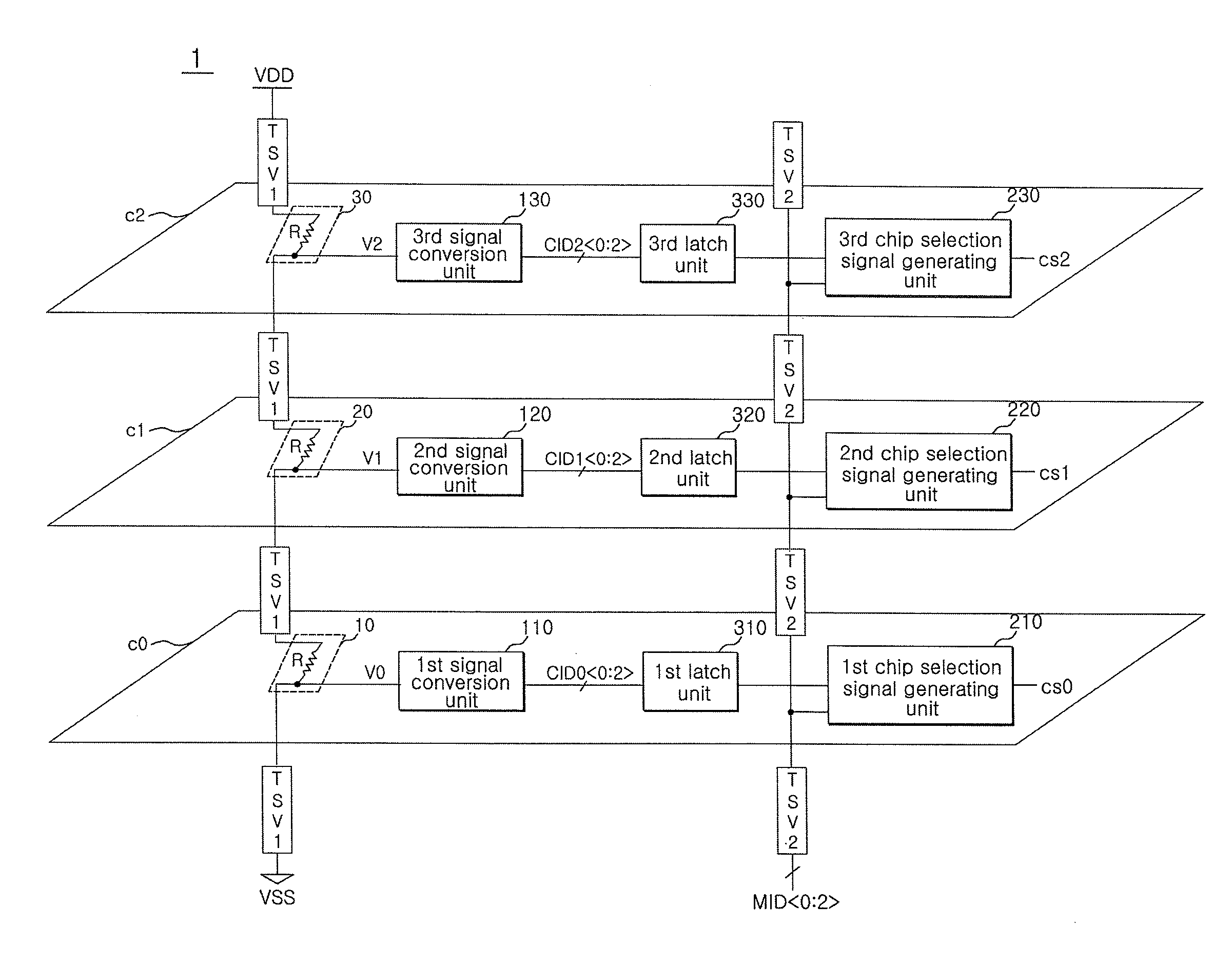
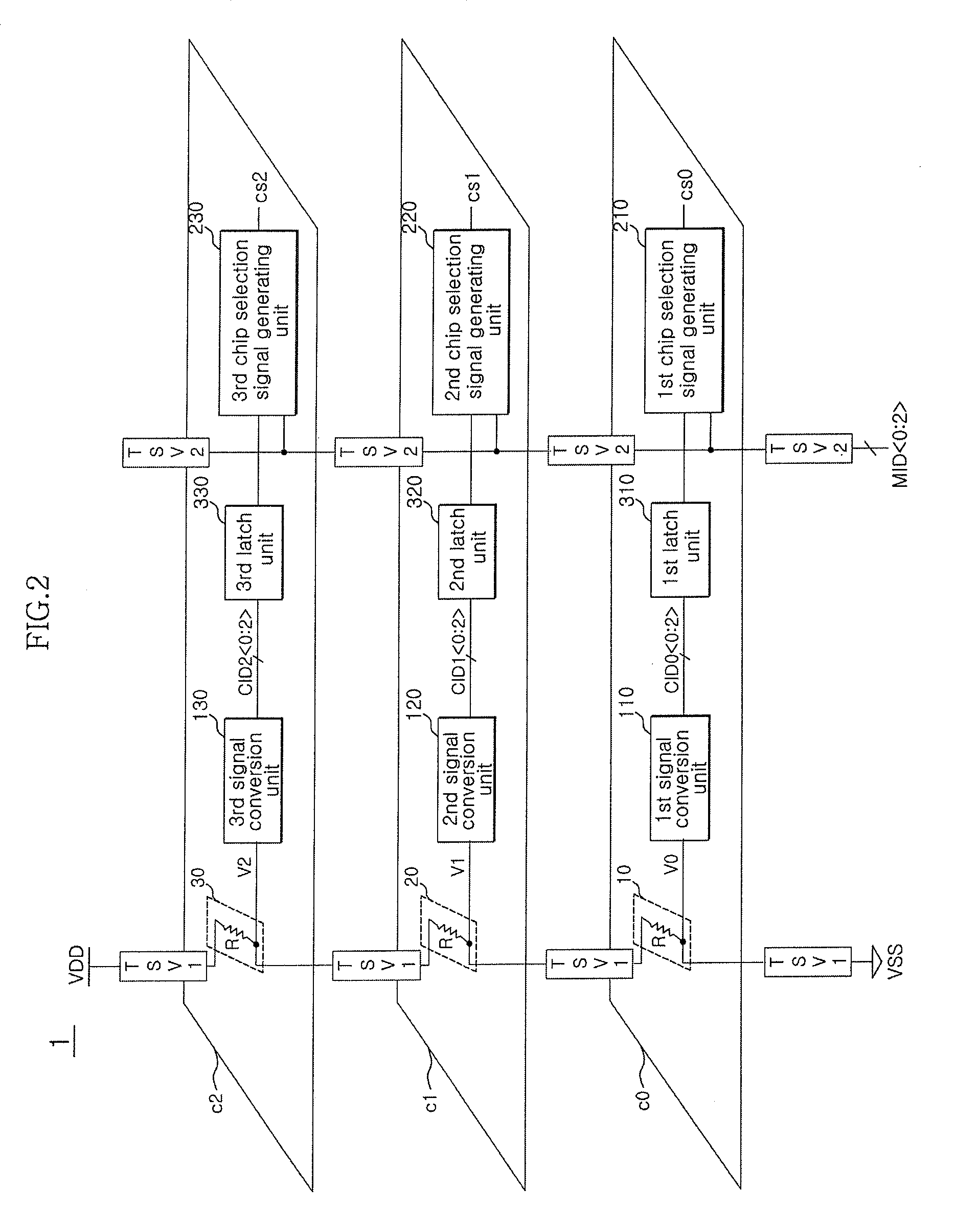
[0016]FIG. 2 is a block diagram schematically showing a configuration of a semiconductor apparatus according to an embodiment of the invention. As shown in FIG. 2, first to third chips c0 to c2 are stacked one on top of another in vertical alignment, and are coupled to each other via a plurality of through silicon vias (TSVs), which constitute the semiconductor apparatus 1. FIG. 2 illustrates a structure of three stacked chips, although the invention is not limited to the specific embodiment. In addition, first and second TSVs TSV1 and TSV2 are shown for the purpose of describing the operation of the semiconductor apparatus 1 in FIG. 2. The first and second TSVs TSV1 and TSV2 penetrate and couple the first to third chips c0 to c2 together.

[0017]Each of the first to third...


PUM


Abstract

A semiconductor apparatus having a plurality of stacked chips includes: a through silicon via (TSV) configured to couple the plurality of chips together and configured to be coupled in series to a plurality of voltage drop units; a plurality of signal conversion units, each of which is configured to convert a voltage outputted from the voltage drop unit of the corresponding one of the plurality of chips to a digital code signal and provide the digital code signal as chip identification signal of the corresponding one of the plurality of chips; and a plurality of chip selection signal generating units, each of which is configured to compare the chip identification signal with a chip selection identification signal to generate a chip selection signal of the corresponding one of the plurality of chips.

Description

CROSS-REFERENCE TO RELATED APPLICATION[0001]The present application claims priority under 35 U.S.C. §119(a) to Korean Application No. 10-2009-0103596, filed on Oct. 29, 2009, which is incorporated by reference in its entirety as if set forth in full.BACKGROUND[0002]1. Technical Field[0003]Various aspects of the present disclosure generally relate to a semiconductor memory apparatus, and more particularly, to a semiconductor apparatus including a chip selection circuit.[0004]2. Related Art[0005]In an effort to increase an integration density of a semiconductor apparatus, a three-dimensional (3D) semiconductor apparatus that stacks and packages a plurality of chips into a single package is recently being developed. Since the 3D semiconductor apparatus includes multiple chips in a single device, the 3D semiconductor apparatus is configured such that an electrical signal can distinguish each of the plurality of chips from other chips and select a specific chip from the plurality of chip...

Claims


Application Information

Patent Timeline
Patent Type & Authority Patents(United States)
IPC IPC(8): G11C5/02
CPCG11C5/04H01L24/73H01L25/0657H01L2224/16145H01L2224/48091H01L2924/01006H01L2225/06513H01L2225/06541H01L2924/01033H01L2224/48227H01L2924/00014G11C5/14G11C8/12
Inventor JIN, SIN HYUNLEE, JONG CHERN
Owner SK HYNIX INC
Why Eureka
Try Eureka