Semiconductor device and display device

a display device and semiconductor technology, applied in static indicating devices, instruments, optics, etc., can solve the problems of defective display, significant defective display, etc., to suppress the voltage drop in the power supply line, prevent the effect of defective display, and reduce the resistance of the power supply lin

Inactive Publication Date: 2006-11-02
SEMICON ENERGY LAB CO LTD
View PDF8 Cites 122 Cited by
  • Summary
  • Abstract
  • Description
  • Claims
  • Application Information

AI Technical Summary

Benefits of technology

[0013] In view of the above, it is an object of the present invention to decrease the resistance of a power supply line, to suppress a voltage drop in the power supply line, and to prevent defective display.
[0028] Note that a switch to be described in the present invention can be of various types, one example of which is an electric switch, a mechanical switch, or the like. In other words, any switch that can control current flow can be used, and various kinds of switches can be used without limitation to a specific switch. For example, the switch may be a transistor, a diode (such as a PN diode, a PIN diode, a Schottky diode, or a diode-connected transistor), or a logic circuit that is a combination thereof. In the case of using a transistor as the switch, the transistor operates as a mere switch. Therefore, the polarity (conductivity type) of the transistor is not particularly limited. However, in the case where less off-current is desired, it is desirable to use a transistor having a polarity with less off-current. As the transistor with small off-current, a transistor provided with an LDD region, a transistor having a multi-gate structure, or the like can be used. In addition, it is desirable to use an n-channel transistor in the case where a transistor to be operated as a switch operates in a state where a potential of a source terminal thereof is close to a lower potential side power source (such as Vss, GND, or 0V), whereas it is desirable to use a p-channel transistor in the case where a transistor operates in a state where a potential of a source terminal thereof is close to a higher potential side power source (such as Vdd). This is because an absolute value of a gate-source voltage can be increased, so that the transistor easily operates as a switch. Note that the switch may be of CMOS type using both an n-channel transistor and a p-channel transistor. If the switch is of CMOS type, it can operate appropriately even in the case where conditions vary, for example, a voltage to be outputted through the switch (in other words, an input voltage to the switch) is higher or lower than an output voltage.
[0034] Defective display can be prevented by decreasing the resistance of a power supply line and suppressing a voltage drop in the power supply line.

Problems solved by technology

Therefore, there is a significant voltage drop in the power supply line if the resistance of the power supply line is high.
As a result, a power supply potential inputted to the pixel and the peripheral driver circuit is decreased, which causes defective display.
In particular, an increase in contact resistance of the connection terminal to which a power supply potential serving as a power source is inputted is a cause of defective display.

Method used


Image

  • Semiconductor device and display device
  • Semiconductor device and display device
  • Semiconductor device and display device

Examples


embodiment mode 1

[0122] In this embodiment mode, the case of applying the present invention to a display panel is explained. In addition, in this embodiment mode, a structure in which a composite connection terminal includes a composite connection pad is explained. In other words, explanation is made on a structure in which a composite connection terminal includes one connection pad (composite connection pad) and the composite connection pad is electrically connected to a plurality of FPC pads through an anisotropic conductive film.

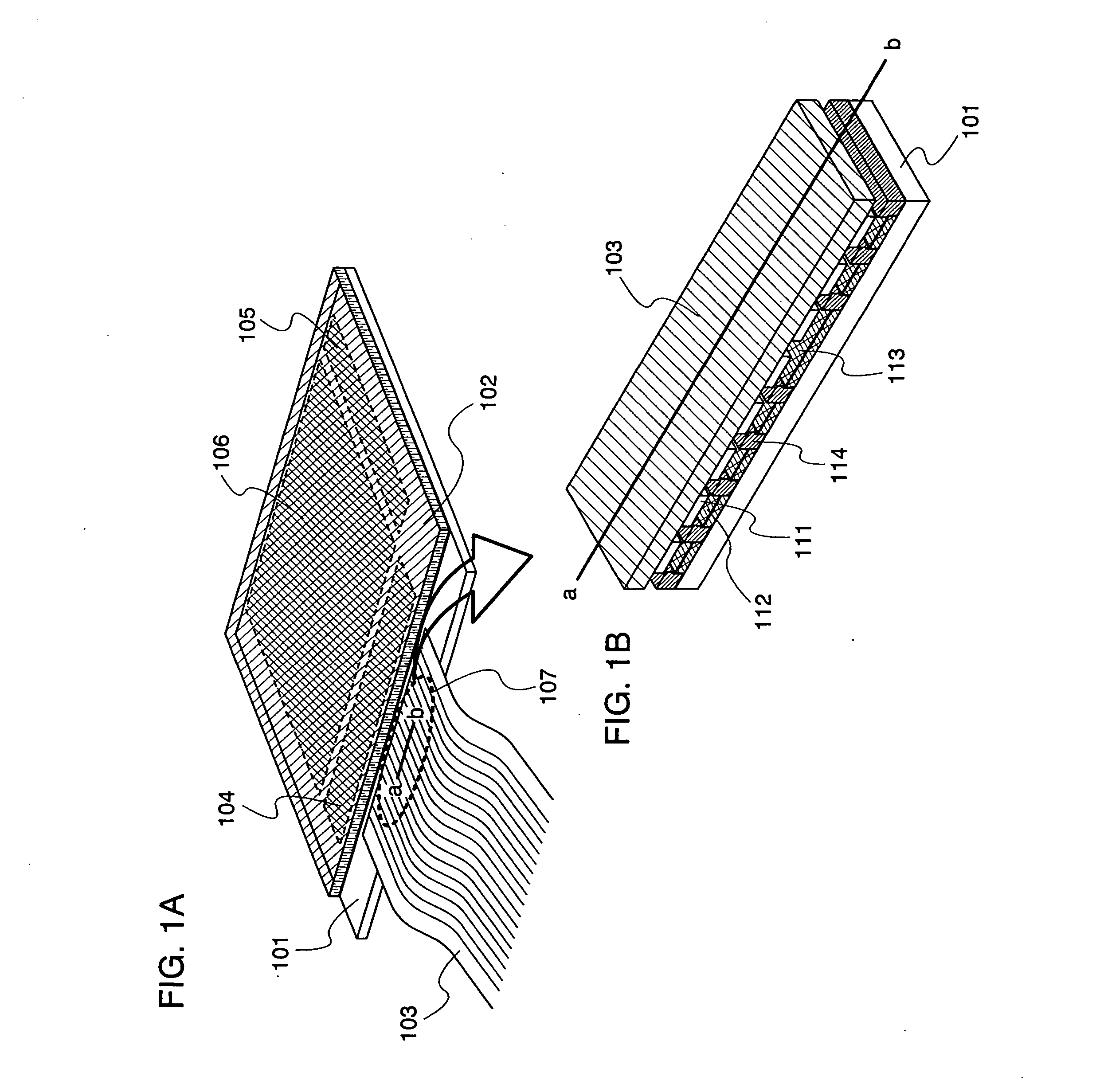
[0123] First, a module in which a display panel is connected to an FPC in this embodiment mode is shown in FIG. 1A. Note that such a module and a main body of a display panel are collectively referred to as a display device in this specification.

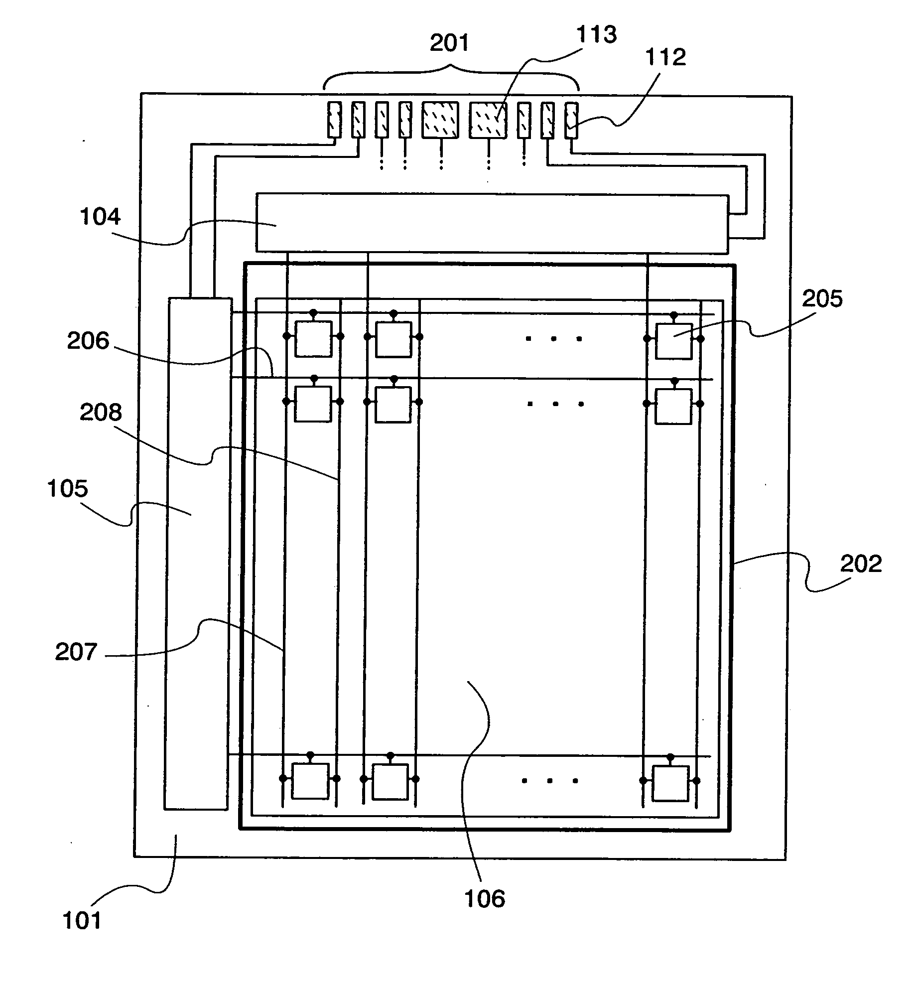
[0124] A pixel portion 106 and peripheral driver circuits (a scan line driver circuit 105 and a signal line driver circuit 104) for driving the pixel portion 106 are formed over a substrate 101. Then, the substrate 101 is attach...

embodiment mode 2

[0149] In this embodiment mode, structures of the connection pads (the reference connection pad 112 and the composite connection pad 113) which are part of the connection terminals (the reference connection terminal and the composite connection terminal) described in Embodiment Mode 1 and a wire extending from the connection pads into a sealing region are explained in detail.

[0150] Note that the display panel to be described in this embodiment mode is particularly suitable for a display panel having a structure in which peripheral driver circuits (a scan line driver circuit and a signal line driver circuit) for driving a pixel are integrated with a pixel portion. In other words, the peripheral driver circuit includes a thin film transistor (also referred to as a TFT) and the like formed at the same time as the formation of a thin film transistor included in the pixel. A schematic diagram of a display panel having such a structure is shown in FIG. 9. Note that the connection termina...

embodiment mode 3

[0171] In this embodiment mode, a structure of a display device is explained. In particular, explanation is made in this embodiment mode, focusing on the connection structure between a composite connection pad and an opposite electrode.

[0172] First, a first structure of this embodiment mode is explained with reference to FIG. 13. Note that components in common with FIG. 2 are denoted by common reference numerals, and explanation thereof is omitted. In the first structure, a wide wire 1301 which is part of the opposite electrode 202 is formed across the signal line driver circuit 104, and is connected to a wire extending from the composite connection pad 113 through a contact hole 1302. In this case, the wide wire 1301 is preferably formed to be wider than the line width of the composite connection pad 113. Then, contact resistance can be decreased since the contact hole 1302 can be enlarged. In other words, as shown in FIG. 45, the wire 1204 extending from the composite connection ...


PUM


Abstract

If misalignment in a line width direction of an electrode (pad) of a connection terminal is caused in attachment of a substrate and an FPC, a connection area of the FPC terminal and the connection terminal becomes smaller and contact resistance is increased. In particular, an increase in contact resistance of the connection terminal to which a power supply potential serving as a power source is inputted is a cause of defective display. In view of the above, an object of the present invention is to decrease the resistance of a power supply line, to suppress a voltage drop in the power supply line, and to prevent defective display. A connection terminal portion includes a plurality of connection terminals. The plurality of connection terminals is provided with a plurality of connection pads which is part of the connection terminal. The plurality of connection pads includes a first connection pad and a second connection pad having a line width different from that of the first connection pad. Pitches between the plurality of connection pads are equal to each other.

Description

BACKGROUND OF THE INVENTION [0001] 1. Field of the Invention [0002] The present invention relates to a semiconductor device including a connection terminal. In particular, the invention relates to a structure of a connection terminal of a display device including a pixel portion where pixels are arranged in matrix, and to a connection structure between an external terminal and a connection terminal of a display device. [0003] 2. Description of the Related Art [0004] A display device may have a structure in which a flexible printed circuit is conductively connected to a display panel and a signal and power are supplied through the flexible printed circuit to the display panel. [0005] For example, the display panel includes a pixel portion and a peripheral driver circuit for driving the pixel portion over a substrate, and the substrate is attached to an opposite substrate with a sealant in a sealing region. Then, at least the pixel portion is sealed with the substrate, the opposite su...

Claims


Application Information

Patent Timeline
Patent Type & Authority Applications(United States)
IPC IPC(8): G09G5/00
CPCG02F1/13452G09G3/20G09G2300/0426H05K1/0263H05K1/0265H05K1/117H01L2924/0002H05K3/361H05K2201/094H05K2201/09727H01L2924/00G02F1/13306G02F1/133345G02F1/133512G02F1/133514G02F1/1339G02F1/13394G02F1/1341G02F1/1368G09G3/2092G09G3/3614G09G2300/0408G09G2300/0439G09G2300/08G09G2310/0264G09G2320/043G09G2330/021G09G2330/08H01L27/1222H05K1/148H05K2201/10136H05K2201/10166
Inventor KIMURA, HAJIMEYAMAZAKI, SHUNPEI
Owner SEMICON ENERGY LAB CO LTD
Why Eureka
Try Eureka