Display with organic light emitting elements including a light emitting layer provided by transferring a transfer layer from a donor substrate to an acceptor substrate

a technology of light emitting elements and organic light, applied in the field of display, can solve the problems of streaking unevenness, uneven light, and so on, and achieve the effect of enhancing display quality and suppressing the distribution of film thickness

Inactive Publication Date: 2012-07-31
SONY CORP
View PDF9 Cites 8 Cited by
  • Summary
  • Abstract
  • Description
  • Claims
  • Application Information

AI Technical Summary

Benefits of technology

[0007]The present application in an embodiment provides a display that has suppressed distribution of t...

Problems solved by technology

Furthermore, there is a fear that so-called reverse transfer occurs in the transfer step as shown in FIG. 30A.
This cu...

Method used


Image

  • Display with organic light emitting elements including a light emitting layer provided by transferring a transfer layer from a donor substrate to an acceptor substrate
  • Display with organic light emitting elements including a light emitting layer provided by transferring a transfer layer from a donor substrate to an acceptor substrate
  • Display with organic light emitting elements including a light emitting layer provided by transferring a transfer layer from a donor substrate to an acceptor substrate

Examples


working examples

[0090]Specific working examples of the present invention will be described below.

working example 1

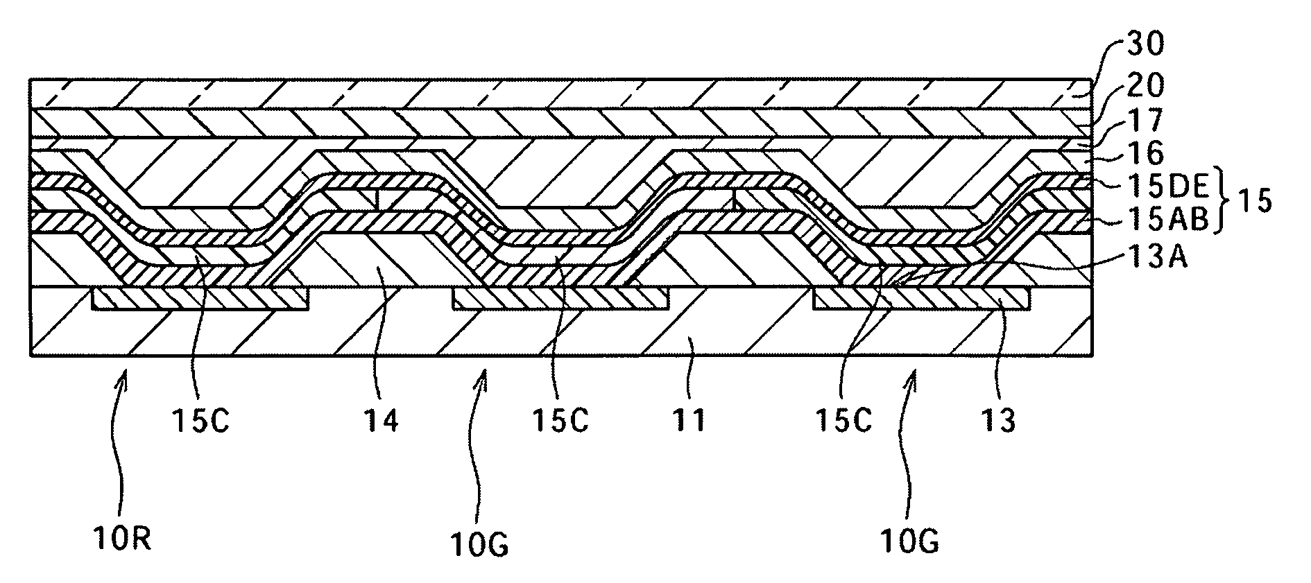
[0091]Similarly to the first embodiment, a display including the red and blue organic light-emitting elements 10R and 10B was fabricated. In this fabrication, the width of the light-emission area 13A and the distances CC and DD were measured. As a result, the width of the light-emission area 13A was 70 μm, and the distances CC and DD were 78 μm and 122 μm, respectively. The light-emitting latter 15C was formed bad transfer for each of the organic light-emitting elements 10R and 10B. The length of the longitudinal axis of the beam spot of laser light was varied to various values in the range of 70 μm to 130 μm, so that the width W of the light-emitting layer 15C along the row direction was varied to various values in the range of 70 μm to 130 μm. The shorter axis of the beam spot of the laser light was fixed to 20 μm, and the laser light was moved for scanning in the direction perpendicular to the longitudinal direction of the beam spot of the laser light. The wavelength and energy d...

working example 2

[0092]A display was fabricated in the same manner as that of Working example 1, except that the rib 14A shown in FIG. 10 was formed on the top surface of the insulating layer 14 and the distances CC and DD were set to 82 μm and 118 μm, respectively.

[0093]Regarding the displays obtained as Working examples 1 and 2, the distribution of the Film thickness of the light-emitting layer 15C in the light-emission area 13A of the organic light-emitting element 10R and the light-emission efficiency of the organic light-emitting element 10B were investigated. The results are shown in FIG. 22.

[0094]As is apparent from FIG. 22, if the light-emitting layer 15C did not include C, i.e., if the width W of the light-emitting layer 15C along the row direction was smaller than the distance CC, the distribution of the film thickness of the light-emitting layer 15C in the light-emission area 13A of the organic light-emitting element 10R was significantly wide. This causes in-plane luminance unevenness an...


PUM


Abstract

A display is provided. The display includes an acceptor substrate including red light-emitting elements arranged in a first column, green light-emitting elements arranged in a second column, and blue light-emitting elements arranged in a third column. The light-emitting elements are arranged along a row direction and are each obtained by arranging rectangular organic light-emitting elements for generating light of one of red, green, and blue along a longitudinal direction of the organic light-emitting elements.

Description

CROSS REFERENCES TO RELATED APPLICATIONS[0001]The present application claims priority related to Japanese Patent Application JP 2007-064787 filed in the Japan Patent Office on Mar. 14, 2007, the entire contents of which being incorporated herein by reference.BACKGROUND[0002]The present application relates to a display that employs organic light-emitting elements having a transferred light-emitting layer obtained by a thermal transfer method.[0003]As one of manufacturing methods for an organic light-emitting element, a pattern fabrication method employing thermal transfer has been disclosed. In the thermal transfer method, a donor component arising from formation of a transfer layer containing a light-emitting material over a support is formed. Subsequently, this donor component is disposed to face an acceptor substrate for forming an organic light-emitting element, and the transfer layer is transferred to the acceptor substrate by irradiation with a radiant ray under a low-pressure ...

Claims


Application Information

Patent Timeline
IPC IPC(8): H01J1/62
CPCH01L27/3211H01L27/3246H01L27/3206H01L51/0013H01L27/3283H01L51/56H10K59/35H10K59/173H10K59/122H10K71/18H10K71/00H10K59/30H10K10/488
Inventor MATSUO, KEISUKESATO, CHIYOKOHANAWA, KOHJISHIBASAKI, TAKANORIYAMAMOTO, TETSUROMIURA, KIWAMU
Owner SONY CORP
Why Eureka
Try Eureka