Using a data cache array as a DRAM load/store buffer

a data cache and array technology, applied in the field of cache systems, can solve the problems of affecting the overall performance of the system, requiring high data throughput, and requiring large amounts of storage space for dirty data and read returns,

Active Publication Date: 2012-07-31
NVIDIA CORP
View PDF3 Cites 24 Cited by
  • Summary
  • Abstract
  • Description
  • Claims
  • Application Information

AI Technical Summary

Benefits of technology

[0010]One advantage of the disclosed method is that allows the intermediate cache to process read and write operations without using separate load and store buffers for data being received from or transmitted to the external memory.

Problems solved by technology

Applications that require high data throughput, such as graphics processing, will require considerable amounts of storage space for dirty data and read returns.
If a system lacks sufficient storage for these operations, then overall performance will be degraded.
One drawback to this approach is that the amount of dedicated space allocated to the read and write data buffers is proportional to the throughput of data in the system.
Since many systems, like graphics processing systems, require very high throughput, implementing intermediate read and write buffers in such systems consumes a large amount of memory space, making such a solution undesirable.

Method used


Image

  • Using a data cache array as a DRAM load/store buffer
  • Using a data cache array as a DRAM load/store buffer
  • Using a data cache array as a DRAM load/store buffer

Examples


Embodiment Construction

[0021]In the following description, numerous specific details are set forth to provide a more thorough understanding of the present invention. However, it will be apparent to one of skill in the art that the present invention may be practiced without one or more of these specific details. In other instances, well-known features have not been described in order to avoid obscuring the present invention.

System Overview

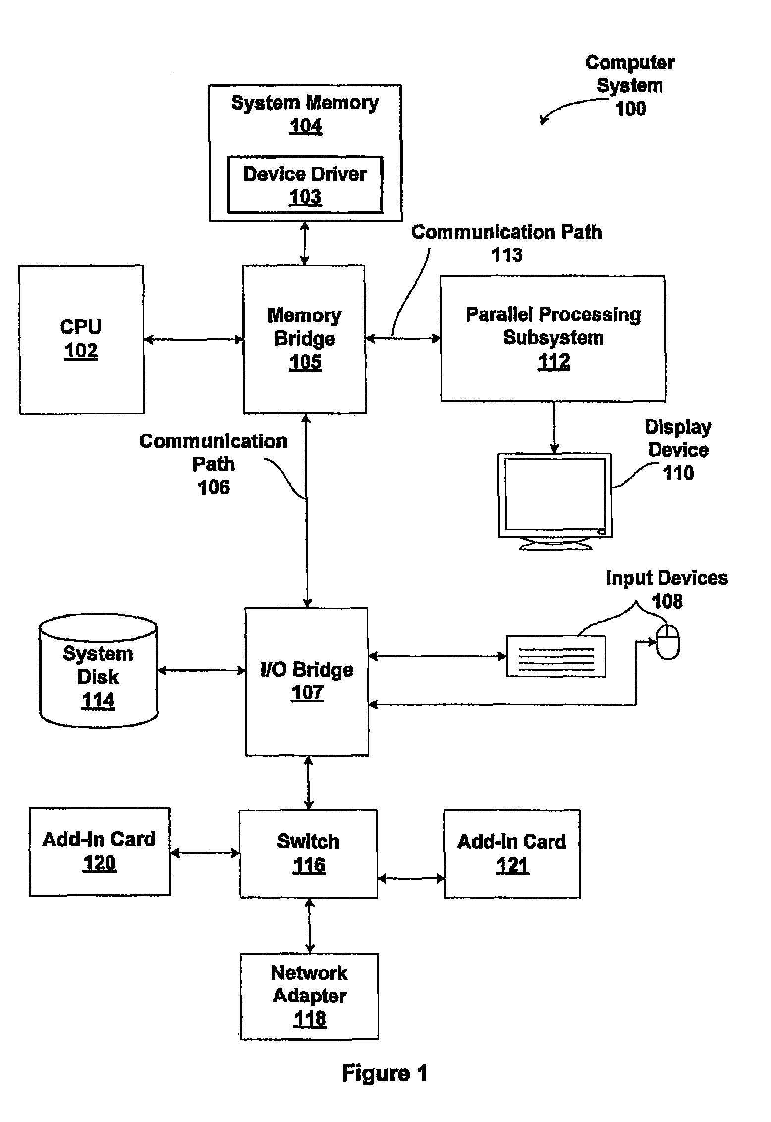
[0022]FIG. 1 is a block diagram illustrating a computer system 100 configured to implement one or more aspects of the present invention. Computer system 100 includes a central processing unit (CPU) 102 and a system memory 104 communicating via a bus path that may include a memory bridge 105. Memory bridge 105, which may be, e.g., a Northbridge chip, is connected via a bus or other communication path 106 (e.g., a HyperTransport link) to an I / O (input / output) bridge 107. I / O bridge 107, which may be, e.g., a Southbridge chip, receives user input from one or more user input ...


PUM


Abstract

One embodiment of the invention sets forth a mechanism for using the L2 cache as a buffer for data associated with read / write commands that are processed by the frame buffer logic. A tag look-up unit tracks the availability of each cache line in the L2 cache, reserves necessary cache lines for the read / write operations and transmits read commands to the frame buffer logic for processing. A data slice scheduler transmits a dirty data notification to the frame buffer logic when data associated with a write command is stored in an SRAM bank. The data slice scheduler schedules accesses to the SRAM banks and gives priority to accesses requested by the frame buffer logic to store or retrieve data associated with read / write commands. This feature allows cache lines reserved for read / write commands that are processed by the frame buffer logic to be made available at the earliest clock cycle.

Description

BACKGROUND OF THE INVENTION[0001]1. Field of the Invention[0002]The present invention relates generally to the field of cache systems and, more specifically, to using a data cache array as a DRAM load / store buffer.[0003]2. Description of the Related Art[0004]One element of a memory subsystem within certain processing units is a Level 2 Cache memory (referred to herein as “L2 cache”). The L2 cache is a large on-chip cache memory that serves as an intermediate point between an external memory (e.g., frame buffer memory) and internal client of the memory subsystem (referred to herein as the “clients”). The L2 cache temporarily stores data that the clients are reading from and writing to the external memory which is often a DRAM.[0005]In such a system, coherency has to be maintained between data present in the L2 cache and the data stored in the external memory. “Dirty data,” that is, data transferred from a client to the L2 cache during a write operation, needs to remain in the on-chip...

Claims


Application Information

Patent Timeline
Patent Type & Authority Patents(United States)
IPC IPC(8): G06F12/00G06F13/28G06F13/00
CPCG06F12/0895
Inventor ROBERTS, JAMESGLASCO, DAVID B.MARCHAND, PATRICK R.HOLMQVIST, PETER B.LYNCH, GEORGE R.EDMONDSON, JOHN H.
Owner NVIDIA CORP
Why Eureka
Try Eureka