

Liquid crystal display device
a liquid crystal display and display device technology, applied in non-linear optics, instruments, optics, etc., can solve the problem of ordinarily difficult manufacture of reverse wavelength dispersion retardation films, and achieve the effect of wide viewing angle range and high contrast ratio
- Summary
- Abstract
- Description
- Claims
- Application Information
AI Technical Summary
Benefits of technology
Problems solved by technology
Method used
Image

Examples
first embodiment
(First Embodiment of the Present Invention)
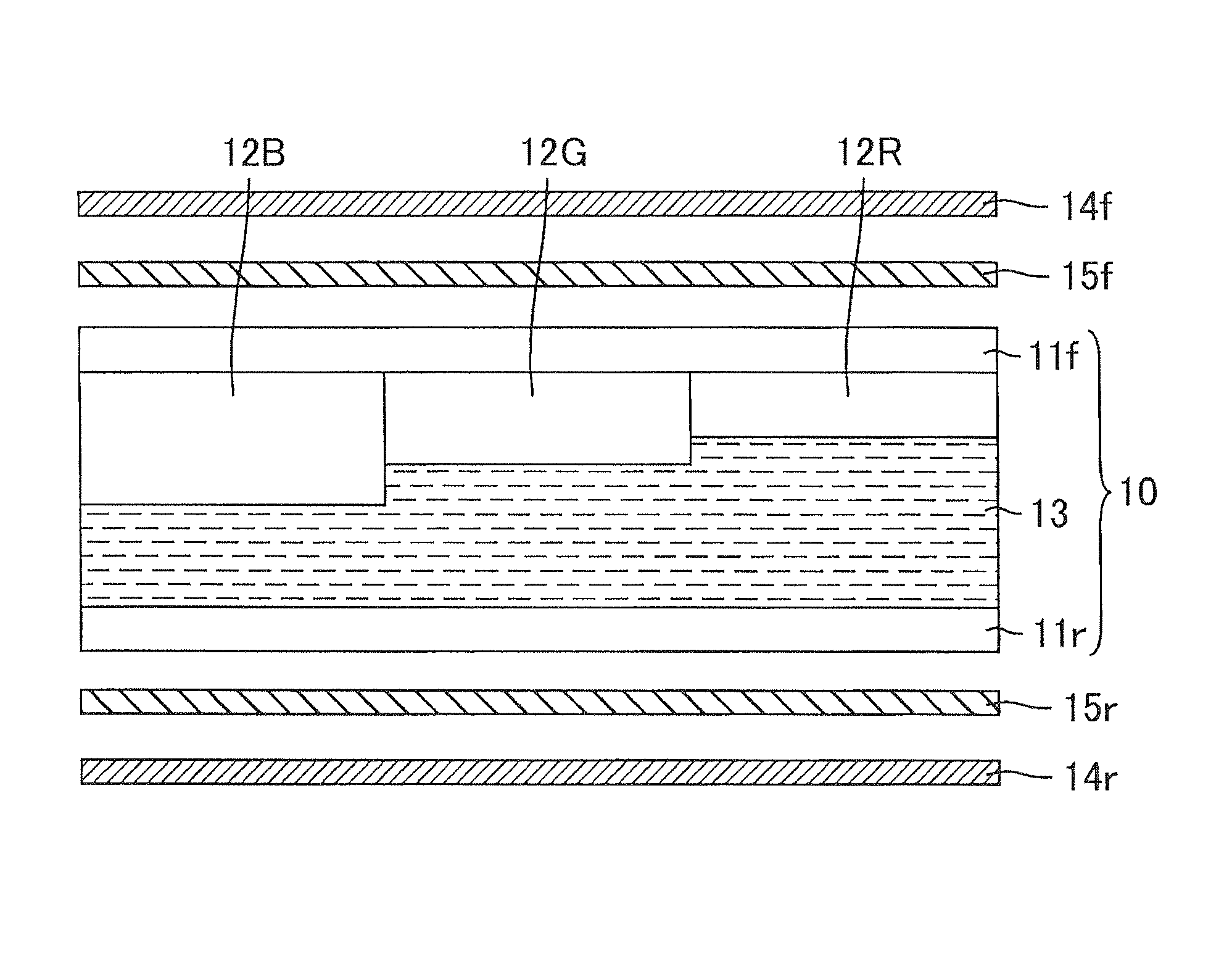
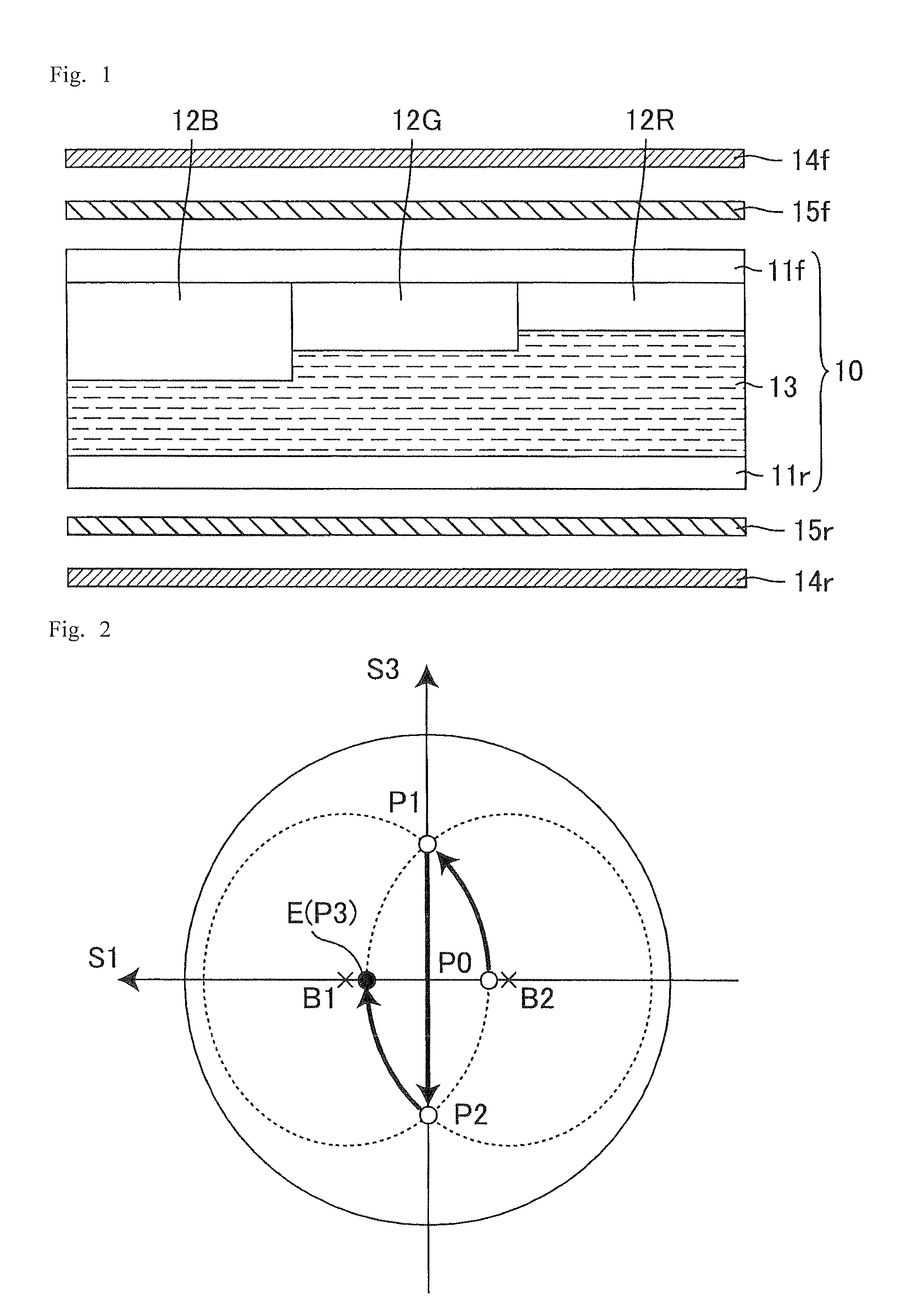
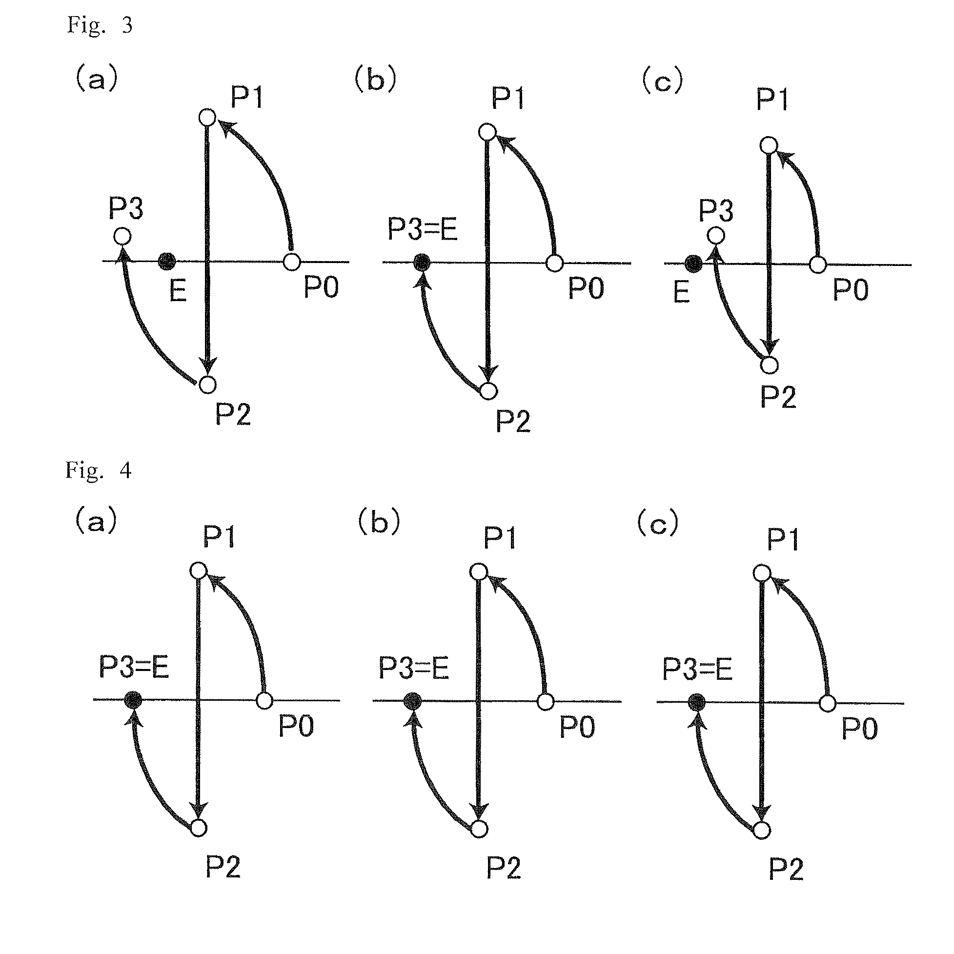
[0042]A first embodiment of the LCD device in which the present invention is used will be explained with reference to FIGS. 1 to 4. FIG. 1 is a cross-sectional schematic diagram illustrating the configuration of an LCD device of a first embodiment of the present invention. FIG. 2 is a diagram for explaining the transition of polarization states in the LCD device of the first embodiment of the present invention, and illustrates a S1-S3 plane in the Poincare sphere. FIG. 3 is a diagram for explaining the transition of polarization states in a conventional LCD device, wherein (a) illustrates an instance of wavelength 450 nm, (b) an instance of wavelength 550 nm, and (c) an instance of wavelength 650 nm. FIG. 4 is a diagram for explaining the transition of polarization states in the LCD device of the first embodiment of the present invention, wherein (a) illustrates an instance of wavelength 450 nm, (b) an instance of wavelength 550 nm, and (c)...
second embodiment
(Second Embodiment of the Present Invention)
[0065]A second embodiment of the LCD device in which the present invention is used will be explained with reference to FIGS. 5 to 7. FIG. 5 is a cross-sectional schematic diagram illustrating the configuration of an LCD device of a second embodiment of the present invention. FIG. 6 is a diagram for explaining the transition of polarization states in the LCD device of the second embodiment of the present invention, and illustrates a S1-S3 plane in the Poincare sphere. FIG. 7 is a diagram for explaining the transition of polarization states in the LCD device of the second embodiment of the present invention, wherein (a) illustrates an instance of wavelength 450 nm, (b) an instance of wavelength 550 nm, and (c) an instance of wavelength 650 nm.
[0066]As illustrated in FIG. 5, the LCD device of the present invention includes a VA LC cell 20; a pair of polarizers 24f, 24r disposed so as to sandwich the LC cell 20; a biaxial retardation film 25r ...
example 1
[0079]Example 1 corresponds to the actual manufacture of an LCD device identical to that of the first embodiment of the present invention. Table 1 summarizes the various optical parameters (retardations and wavelength dispersions thereof) of the LCD device, together with those of Example 2.
PUM
| Property | Measurement | Unit |
|---|---|---|
| wavelengths | aaaaa | aaaaa |
| wavelengths | aaaaa | aaaaa |
| wavelengths | aaaaa | aaaaa |
Abstract
Description
Claims
Application Information