Method for manufacturing a metal gate electrode/high K dielectric gate stack

a technology of dielectric gate stack and metal gate electrode, which is applied in the field of semiconductor technology, can solve the problems of still facing massive challenge to apply the metal gate electrode/high k dielectric stack, still facing massive challenge, and difficult to form a high k dielectric/metal gate electrode gate stack satisfying, etc., to achieve good etching selectivity, improve etching selectivity, and reduce the effect of etching

Active Publication Date: 2012-09-04
INST OF MICROELECTRONICS CHINESE ACAD OF SCI
View PDF7 Cites 4 Cited by
  • Summary
  • Abstract
  • Description
  • Claims
  • Application Information

AI Technical Summary

Benefits of technology

[0005]An object of the present invention is to provide a method for manufacturing a metal gate electrode / high K dielectric gate stack, which provides a steep and anisotropic etching profile of the stack, and has a good etching selectivity with respect to a silicon substrate. The method is also completely compatible with a conventional CMOS process, has a low manufacturing cost, and is easy to be applied to a volume production of the integrated circuit.
[0023]The present invention provides not only a steep etching profile of the stack, but also a good etching selectivity with respect to a silicon substrate. The reason for this is that the BCl3 gas generates not only Cl which reacts with the metal to form a volatile product, but also BOClx which is also a volatile product, and thus BCl3 gas erodes a metal oxide. Moreover, the BCl3 gas can also etch a Hf-based high K material, since the high K material is typically made of a metal oxide. Furthermore, the BCl3 gas reacts with the silicon substrate to form a Si—B bond which passivates the substrate and increases an etching selectivity with respect to the silicon substrate. In the present invention, a mixed gas of BCl3 / Cl2 / Ar / a small amount of O2, is used as an etchant gas for etching the TaN / high K dielectric stack at a high electric field and a low pressure. The inclusion of Cl2 and O2 facilitates formation of a steep etching profile. What's more, the high electric field and the low pressure also facilitate formation of a steep etching profile. The relatively high temperature of the reaction chamber and the electrodes facilitate exhaust of the reaction by-products. By optimizing the powers of the upper and lower electrodes, the pressures and composition of the gases, the present invention achieves a steep etching profile and a good etching selectivity with respect to a silicon substrate. Thus, there is less silicon loss in the process. Moreover, the inventive method is compatible with the conventional CMOS process and has a low manufacturing cost. It overcomes the difficulty in integrating a metal gate / high K dielectric gate stack into the advanced CMOS technology, and is easy to be applied to a volume production of the integrated circuit.

Problems solved by technology

However, it still faces massive challenge to apply the metal gate electrode / high K dielectric stack to the CMOS technology.
In particular, it is difficult to form a high K dielectric / metal gate electrode gate stack satisfying the requirements of device fabrication by etching in the gate-first CMOS process, because an etching rate, an etching selectivity, and an anisotropic etching profile of the gate stack can not be optimized easily at the same time.
Even so, it still faces massive challenge to achieve a steep and anisotropic etching profile of a gate stack and a high etching selectivity to the silicon substrate and the hard mask.

Method used


Image

  • Method for manufacturing a metal gate electrode/high K dielectric gate stack
  • Method for manufacturing a metal gate electrode/high K dielectric gate stack

Examples


Embodiment Construction

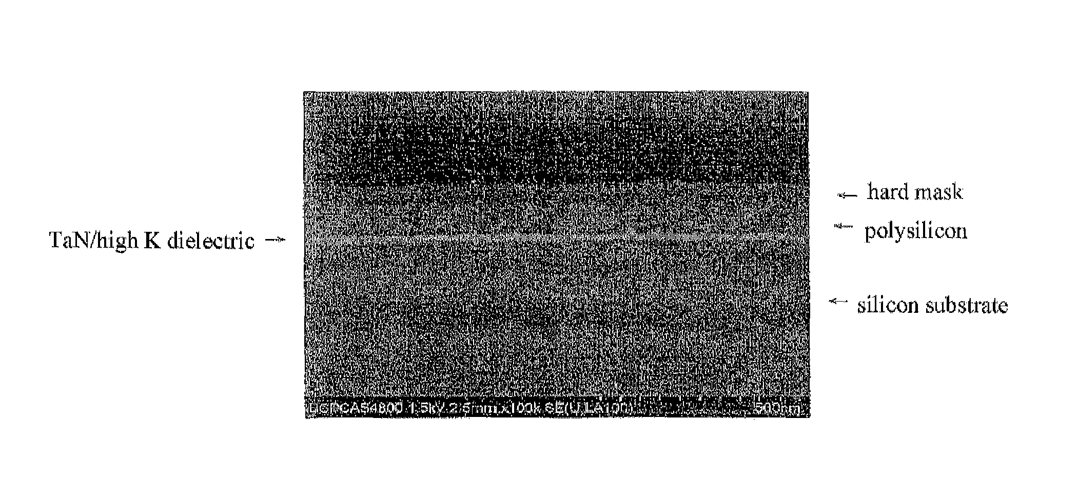
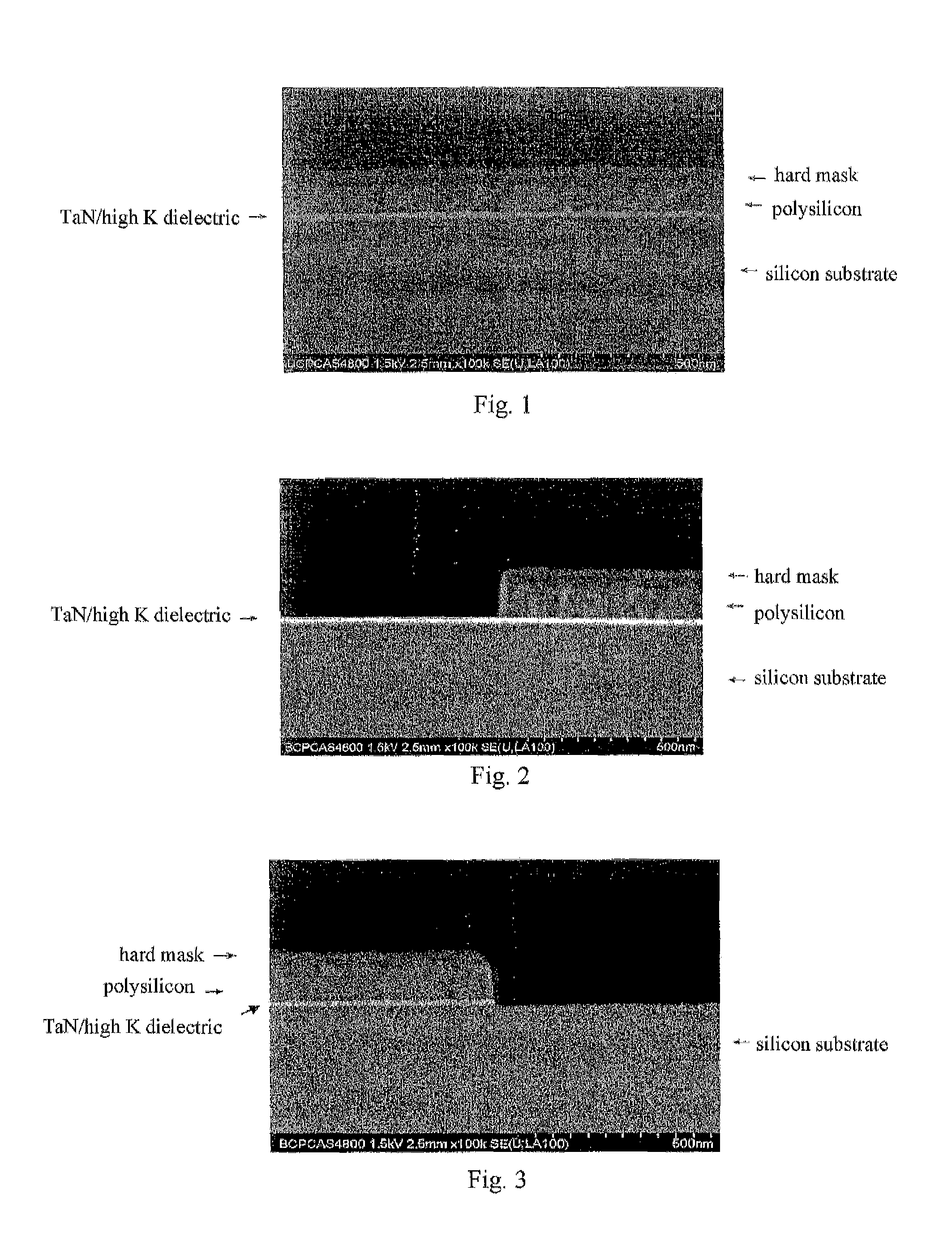
[0027]Aiming at the challenges coming from that the high K dielectric / metal gate electrode new technology must be used in 32 nm / 22 nm technology node, the present invention provides a method for manufacturing a metal gate / high K dielectric gate stack. The invention will be described in connection with the attached drawings so as to clarify its characteristic features. The embodiments given below are illustrative and not to be construed as limiting the invention.

[0028]Step 1) firstly washing a silicon substrate by a conventional process, and then immersing it into a mixed solution of hydrofluoric acid, isopropanol and water in a volume ratio of about 0.2-1.5%:0.01-0.10%:1% for about 2-10 minutes, then rinsing it with deionized water, and drying it by spinning;

[0029]Step 2) forming an interfacial layer of SiON or SiO2 on the silicon substrate, wherein the interfacial layer of SiON may be formed by firstly implanting nitrogen ion and then performing a rapid thermal oxidation, or by fi...


PUM

PropertyMeasurementUnit
etching poweraaaaaaaaaa
operating pressureaaaaaaaaaa

Abstract

A method of manufacturing a metal gate / high K dielectric gate stack includes the steps of: forming an interfacial layer of SiON or SiO2 on a silicon substrate; depositing a high K dielectric film on the interfacial layer; performing a rapid thermal anneal of the high K dielectric film; depositing a TaN metal gate electrode film on the high K dielectric film; depositing a polysilicon gate layer on the TaN metal gate electrode film, and then depositing a hard mask layer; patterning a photoresist mask, and performing an anisotropic etching of the hard mask layer; removing the photoresist mask, and etching the polysilicon by reactive ion etching with the hard mask as masking layer using a mixed gas of Cl2 / HBr; and etching the TaN metal gate electrode / high K dielectric gate stack by reactive ion etching with the hard mask as masking layer using BCl3-based etchant gas.

Description

BACKGROUND OF THE INVENTION[0001]1. Field of Invention[0002]The present invention relates to semiconductor technology, and more particularly, to a method for manufacturing a metal gate electrode / high K dielectric gate stack. The invention can be applied to a high-performance complementary metal-oxide-semiconductor (CMOS) device at 32 nm node and beyond.[0003]2. Description of Prior Art[0004]A dielectric having a high dielectric constant (K) and a metal gate electrode represent a tendency of development while a critical dimension of a CMOS device continue to further scale down. By using a high K dielectric, the gate leakage current can be substantially reduced, because a relatively large physical thickness can be achieved with the same equivalent oxide thickness (EOT). Furthermore, by using a metal gate electrode, a depletion effect of a polysilicon gate electrode and a penetration effect of boron can be eliminated, so that the device has an improved reliability and a reduced gate re...

Claims


Application Information

Patent Timeline
Patent Type & Authority Patents(United States)
IPC IPC(8): H01L21/311
CPCH01L21/28088H01L21/28185H01L21/28202H01L21/2822H01L21/31116H01L21/31122H01L21/32136H01L29/4966H01L29/517
Inventor XU, QIUXIALI, YONGLIANG
Owner INST OF MICROELECTRONICS CHINESE ACAD OF SCI
Why Eureka
Try Eureka