Differential input for ambipolar devices

a technology of ambipolar devices and inputs, applied in pulse manipulation, pulse technique, instruments, etc., can solve the problems of interfering with the desired performance of similar circuits, and the development of circuitry for ambipolar transistors (i.e., transistors b>400/b>) having similar behavior to known circuitry in cmos (or bipolar) can be challenging

Active Publication Date: 2012-09-04
TEXAS INSTR INC
View PDF8 Cites 4 Cited by
  • Summary
  • Abstract
  • Description
  • Claims
  • Application Information

AI Technical Summary

Benefits of technology

[0010]In accordance with a preferred embodiment of the present invention, each ambipolar transistor from the pair of ambipolar tran

Problems solved by technology

While the circuitry of FIG. 1 is well-known and has been used for CMOS transistors for many years, there are emerging technologies that have characteristics that may interfere with the desired performance of similar circu

Method used


Image

  • Differential input for ambipolar devices
  • Differential input for ambipolar devices
  • Differential input for ambipolar devices

Examples


Embodiment Construction

[0026]Refer now to the drawings wherein depicted elements are, for the sake of clarity, not necessarily shown to scale and wherein like or similar elements are designated by the same reference numeral through the several views.

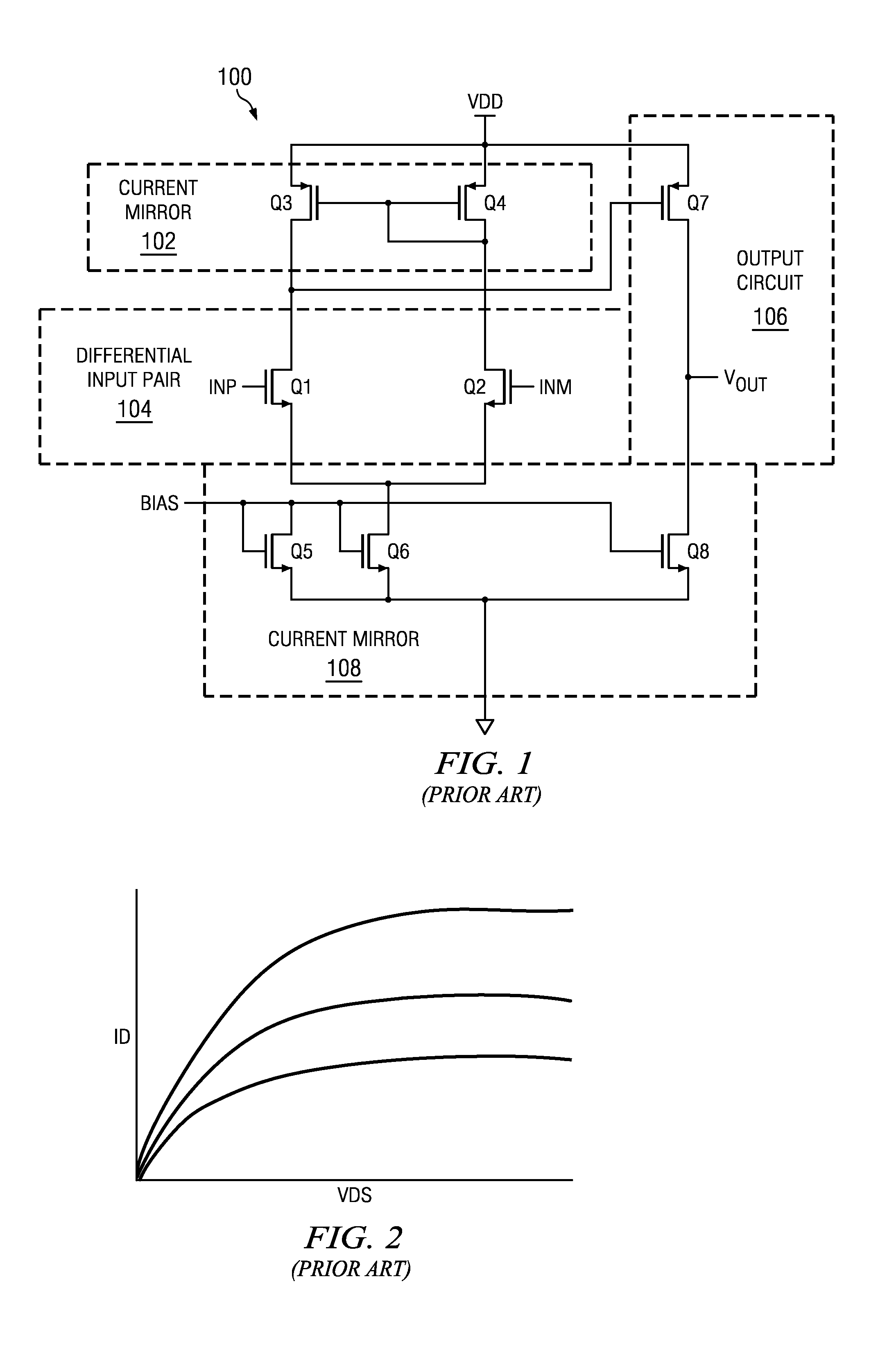
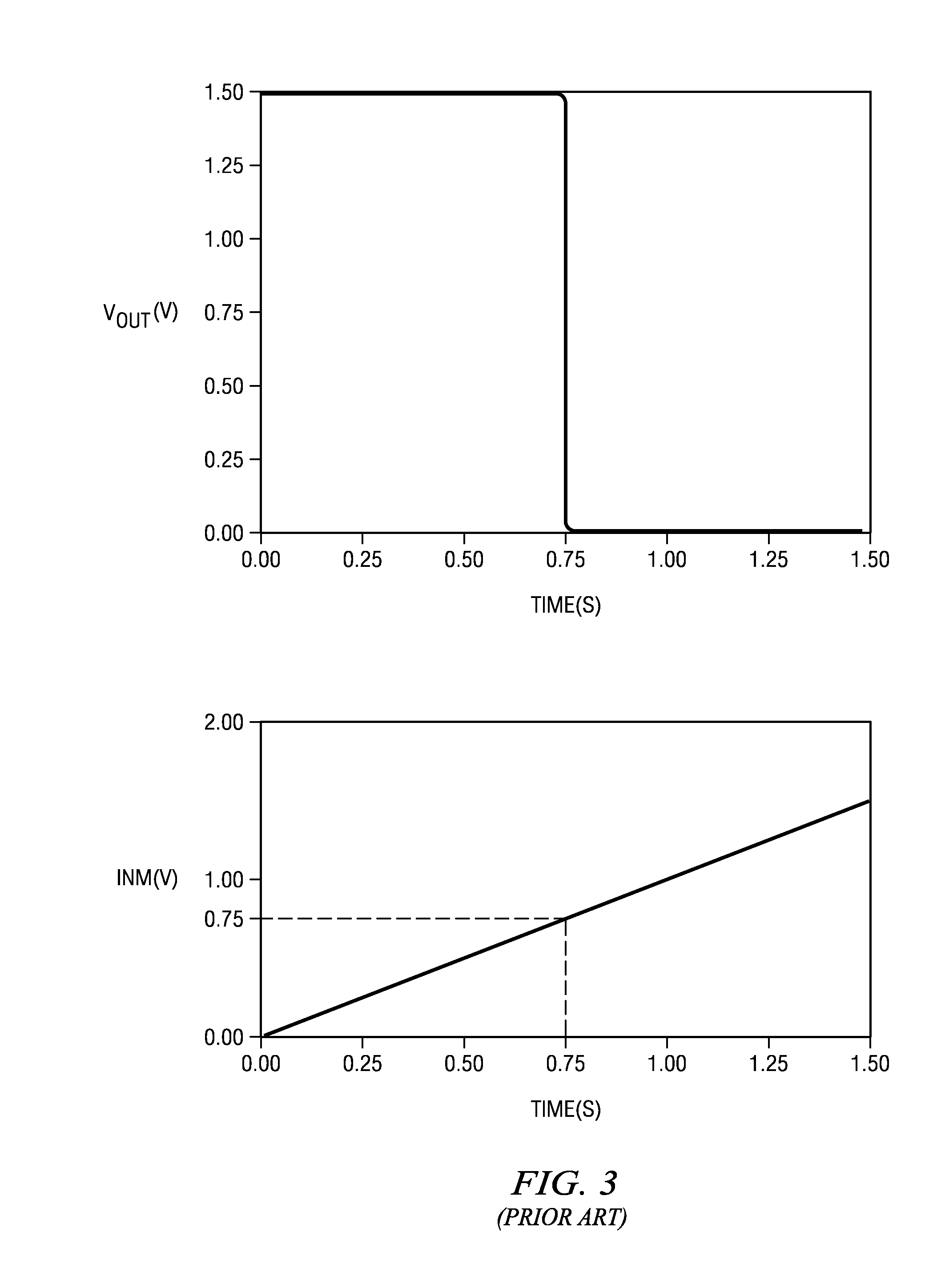
[0027]Turning to FIG. 6, an example of the general operation for amplifier 100 (where transistors Q1 and Q2 have been replaced by ambipolar transistors) can be seen. For this example, the supply voltage VDD is 1.5V and a voltage of 0.75V is applied as signal INP to the ambipolar transistor that replaces transistor Q1. As the voltage for signal INM is ramped, as shown, the output signal VOUT remains 0V until 0.5V is reached. When signal INM reaches 0.5V, output signal VOUT transitions from 0V to 1.5V. The output signal VOUT then transitions back to 0V when signal INM becomes 0.75V. Thus, an amplifier 100 (where transistors Q1 and Q2 have been replaced by ambipolar transistors) does not behave like an ordinary amplifier (i.e., amplifier 100). This unusual behavi...


PUM


Abstract

Differential input pairs have been used in analog electronics with both CMOS and bipolar transistors for many years. Conventional designs for differential input pairs, though, may not be suitable for emerging technology transistors, such as graphene transistors, carbon nanotube (CNT) transistors, or other ambipolar transistors. Here, a differential input pair has been provided that uses ambipolar transistors, which accounts for the more unusual I-V (drain current to gate-source voltage) characteristics of ambipolar transistors.

Description

TECHNICAL FIELD[0001]The invention relates generally to a differential input pair and, more particularly, to a differential input pair that uses ambipolar transistors.BACKGROUND[0002]Turning to FIG. 1, a conventional operational amplifier 100 can be seen. The amplifier 100 generally comprises a current mirrors 102 and 108, a differential input pair 104, and an output circuit 106. The current mirrors 102 and 108 generally and respectively comprise transistors Q3 and Q4 (which, as shown, are PMOS transistors) and transistors Q5, Q6, and Q8 (which, as shown, are NMOS transistors). The differential input pair 104 generally comprises transistors Q1 and Q2 (which, as shown, are NMOS transistors or can be NPN transistors that receive input signal INP and INM). The output circuit 106 generally comprises transistors Q7 (which, as shown, are a PMOS transistor and an NMOS transistor, respectively). Additionally, bias voltage BIAS can be applied to the gates of each of transistors Q5, Q6, and Q...

Claims


Application Information

Patent Timeline
IPC IPC(8): H03F3/45
CPCH03K5/24H03K5/2481H03F3/45183B82Y10/00H01L29/78684H03F2203/45326H03F2203/45674
Inventor MARSHALL, ANDREW
Owner TEXAS INSTR INC
Why Eureka
Try Eureka