Method and apparatus for laser soldering

a laser soldering and laser technology, applied in the direction of metal working apparatus, soldering apparatus, manufacturing tools, etc., can solve the problems of poor appearance, conduction defect, long time for melted solder to spread along the ring-like terminal, etc., and achieve high-quality soldering

Active Publication Date: 2012-09-18
JAPAN UNIX
View PDF18 Cites 2 Cited by
  • Summary
  • Abstract
  • Description
  • Claims
  • Application Information

AI Technical Summary

Benefits of technology

[0008]An object of the invention is to be able to perform the high-quality soldering by eliminating the electronic component burning problem caused by laser beam when a rod terminal of an electronic component is inserted in a through-hole surrounded by a ring-like terminal of a printed circuit board in order to solder the rod terminal and the ring-like terminal using the laser beam.
[0016]According to the invention, the solder paste is previously fed to the ring-like terminal and the rod terminal to fill in the through-hole. Therefore, in the soldering, the laser beam is blocked by the solder paste, and the laser beam cannot pass through the through-hole, which allows the burning problem to be eliminated in the electronic component. In addition to the solder paste, the wire solder is further fed to perform the soldering. Therefore, because the solder paste and the wire solder are fused to cover shortcomings of the solder paste and wire solder, high-quality soldering can be performed.

Problems solved by technology

However, as illustrated in FIG. 7, when a rod terminal 4a of an electronic component 4 is inserted in a through-hole 3 surrounded by a ring-like terminal 2 of a printed circuit board 1 in order to solder the rod terminal 4a and the ring-like terminal 2 using wire solder 5, the laser beam 6 is projected onto the electronic component 4 through a gap 3a between the ring-like terminal 2 and the rod terminal 4a before the wire solder 5 is melted by a laser beam 6 and the through-hole 3 is embedded, which results in a problem in that burning is generated in part of the electronic component 4.
Therefore, due to wettability after melting, unfortunately it takes a long time for the melted solder to spread along the ring-like terminal 2 or the rod terminal 4a or to flow in the through-hole 3.
At this point, 10 when the solder paste is irradiated with the laser beam, the solder paste located outside the ring-like terminal is left while not melted, and the solder paste is scattered around, which easily causes a poor appearance and a conduction defect.
Further, because the large amount of solder paste is fed, not only it takes a long time for the solder paste to be melted with the laser beam, but also the granular paste in the solder paste flowing previously in the through-hole is not completely melted to leave the granular paste.
Therefore, a soldering defect is frequently generated.

Method used


Image

  • Method and apparatus for laser soldering
  • Method and apparatus for laser soldering
  • Method and apparatus for laser soldering

Examples


Embodiment Construction

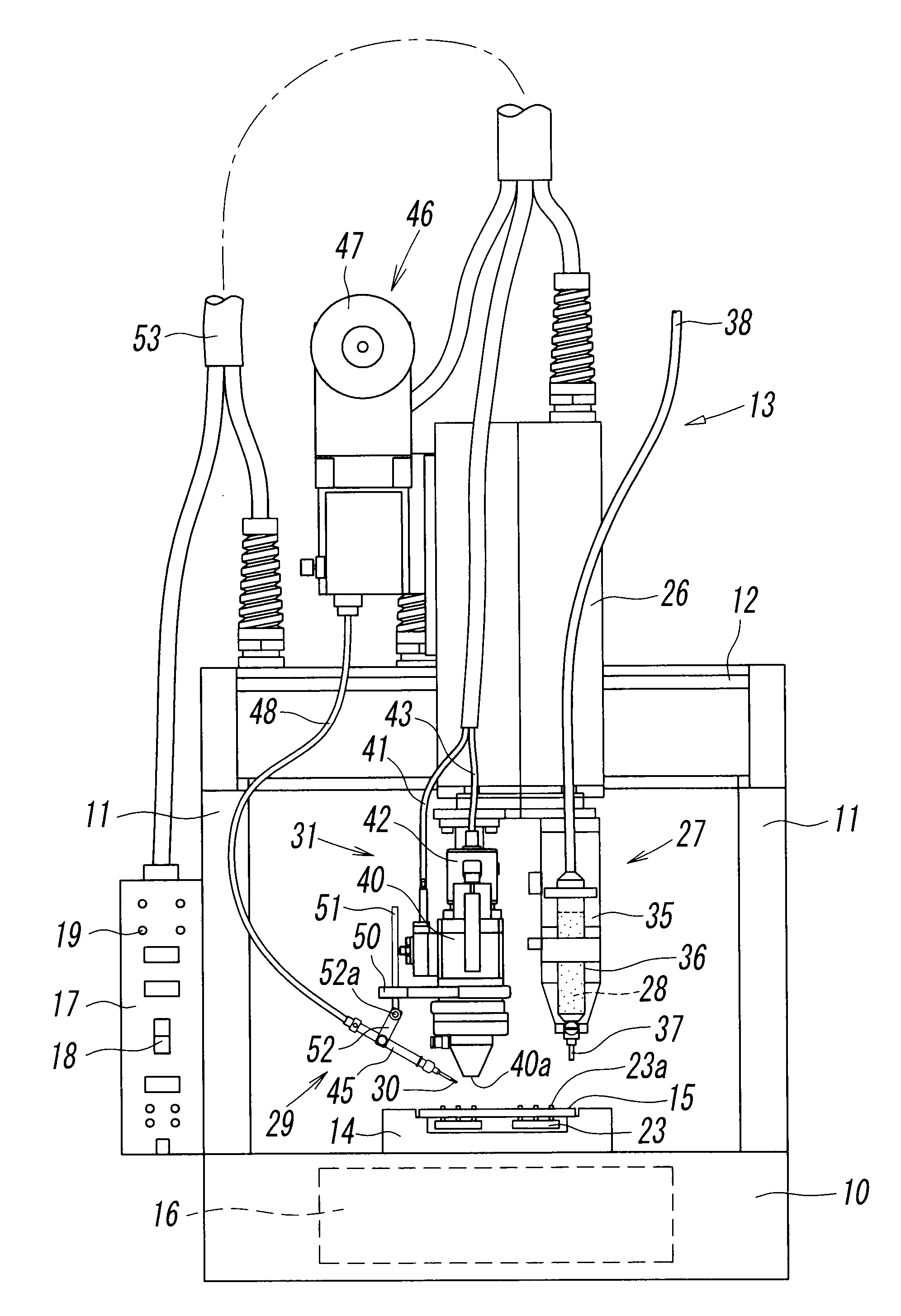
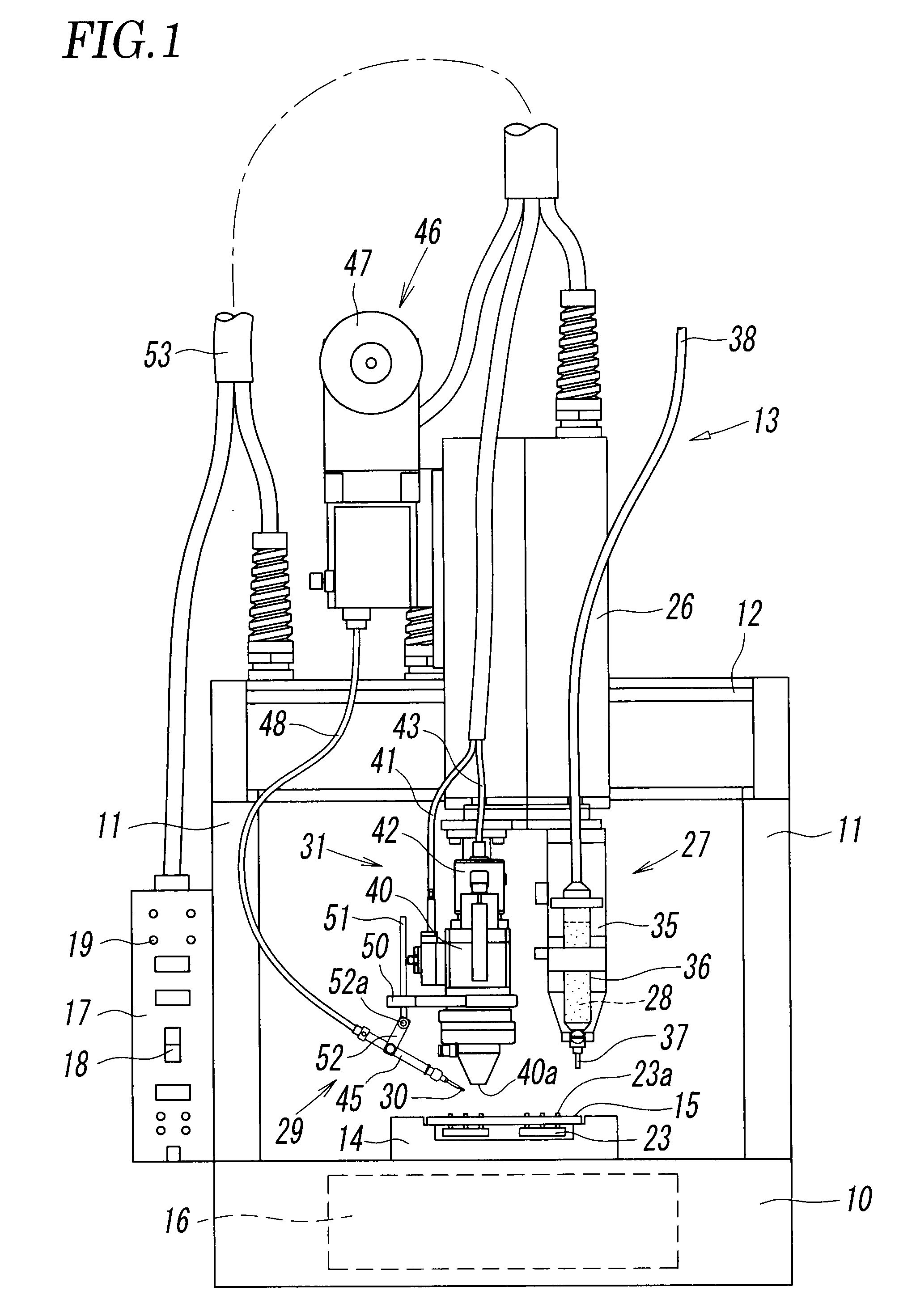
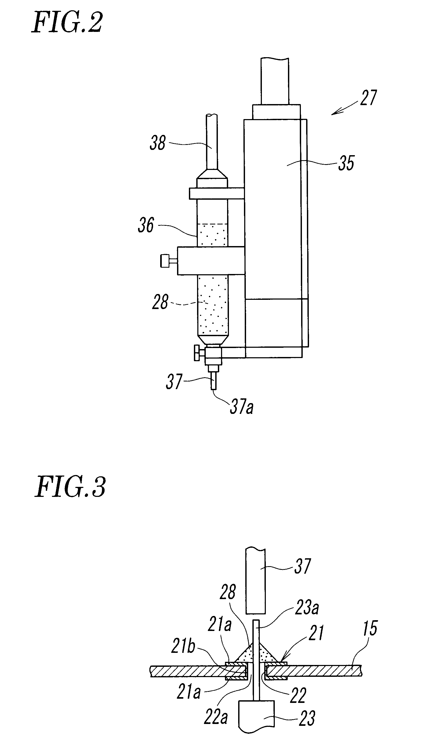
[0024]FIG. 1 is a front view illustrating a laser soldering apparatus according to an embodiment of the invention. The laser soldering apparatus of the embodiment automatically performs the soldering according to a setting program. The laser soldering apparatus includes a base 10 that has a rectangular shape in a planar view, a pair of support pillars 11 that is provided at right and left ends of the base 10, a guide rail 12 that is horizontally bridged between upper end portions of the support pillars 11, a soldering head 13 that is movable along the guide rail 12 in a horizontal direction (X-direction), and a board support table 14 that is disposed on the base 10 in order to place a printed circuit board 15 that is of a soldering target. The board support table 14 is movable in a back-and forth direction (Y-direction) of the base 10 by manipulation.

[0025]A control device 16 is incorporated in the base 10 in order to control an operation of the whole apparatus. A console panel 17 i...


PUM

PropertyMeasurementUnit
time lagaaaaaaaaaa
timeaaaaaaaaaa
wettabilityaaaaaaaaaa

Abstract

In accordance with an aspect of the invention, a solder paste feeding device feeds solder paste to a ring-like terminal surrounding a through-hole and a rod terminal fitted in the through-hole so as to fill in the through-hole, the laser beam irradiation device irradiates the solder past with a laser beam, and wire solder is further fed from above the solder past at the same time as melting of the solder paste is started, thereby fusing the wire solder and the solder paste to solder the ring-like terminal and the rod terminal.

Description

BACKGROUND OF THE INVENTION[0001]1. Field of the Invention[0002]The present invention relates to a technique of soldering electronic components such as IC and LSI to a printed circuit board using a laser beam.[0003]2. Description of the Related Art[0004]The technique of soldering the electronic components such as IC and LSI to the printed circuit board using the laser beam is well known (for example, see Japanese patent Application Laid-open Nos. 4-52073 and 2002-1521). In the technique, the printed circuit board is irradiated with the laser beam from a soldering head of a soldering apparatus, and the solder is melted by heat of the laser beam to perform the soldering. Advantageously the soldering can be performed in a non-contact manner.[0005]However, as illustrated in FIG. 7, when a rod terminal 4a of an electronic component 4 is inserted in a through-hole 3 surrounded by a ring-like terminal 2 of a printed circuit board 1 in order to solder the rod terminal 4a and the ring-like t...

Claims


Application Information

Patent Timeline
Patent Type & Authority Patents(United States)
IPC IPC(8): B23K26/20B23K1/00B23K1/005B23K3/06B23K101/42H05K3/34
CPCB23K1/0016B23K1/0056B23K3/063B23K3/0638B23K3/082B23K3/087B23K26/03H05K3/3447B23K2201/42H05K3/3484H05K3/3494H05K2203/0405H05K2203/107B23K2101/42H05K3/3485
Inventor MATSUSHITA, KOTARO
Owner JAPAN UNIX
Why Eureka
Try Eureka