Supercharge Your Innovation With Domain-Expert AI Agents!

Exposed interconnect for a package on package system

a technology of exposed interconnects and package systems, applied in the direction of electrical apparatus contruction details, printed circuit non-printed electric components association, semiconductor/solid-state device details, etc., can solve the problems of not adequately addressing cooling and reliability concerns, current packaging suppliers are struggling to accommodate high-speed computer devices, and no clear cost-effective technology has yet been identified

Active Publication Date: 2012-09-18
STATS CHIPPAC LTD
View PDF32 Cites 17 Cited by
  • Summary
  • Abstract
  • Description
  • Claims
  • Application Information

AI Technical Summary

Benefits of technology

This approach enables efficient, cost-effective, and reliable signal routing, addressing the challenges of high-speed devices by providing a robust and compact packaging solution that reduces production time and improves performance while meeting competitive pressures.

Problems solved by technology

Current packaging suppliers are struggling to accommodate the high-speed computer devices that are projected to exceed one TeraHertz (THz) in the near future.
The current technologies, materials, equipment, and structures offer challenges to the basic assembly of these new devices while still not adequately addressing cooling and reliability concerns.
The envelope of technical capability of next level interconnect assemblies are not yet known, and no clear cost effective technology has yet been identified.
These challenges demand not only automation of manufacturing, but also the automation of data flow and information to the production manager and customer.
The limitations and issues with current technologies include increasing clock rates, EMI radiation, thermal loads, second level assembly reliability stresses and cost.
As these package systems evolve to incorporate more components with varied environmental needs, the pressure to push the technological envelope becomes increasingly challenging.
More significantly, with the ever-increasing complexity, the potential risk of error increases greatly during manufacture.
Solutions to these problems have been long sought but prior developments have not taught or suggested any solutions and, thus, solutions to these problems have long eluded those skilled in the art.

Method used


Image

  • Exposed interconnect for a package on package system
  • Exposed interconnect for a package on package system
  • Exposed interconnect for a package on package system

Examples


first embodiment

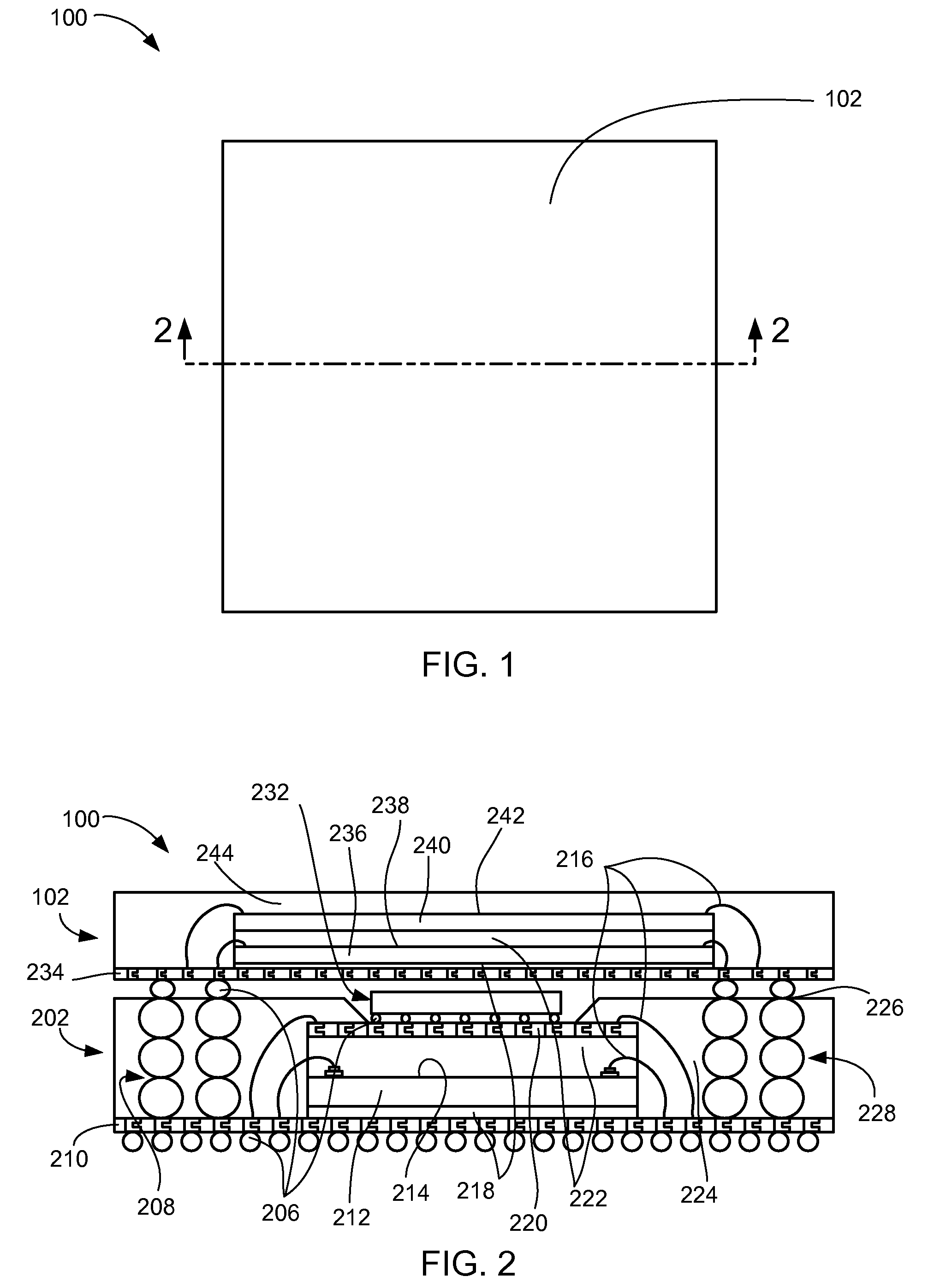
[0028]Referring now to FIG. 1, therein is shown a top view of an integrated circuit package system 100 in the present invention. The integrated circuit package system 100 is shown having a package such as a second package 102.

[0029]Referring now to FIG. 2, therein is shown a cross-sectional view of the integrated circuit package system 100 along the line 2-2 of FIG. 1. The integrated circuit package system 100 is shown having a first package 202 with the second package 102 mounted above.

[0030]The second package 102 is connected to the first package 202 with interconnects such as solder balls 206. The solder balls 206 connecting the first package 202 to the second package 102 are connected to exposed interconnects 208. The exposed interconnects 208 may be solder balls, conductive pins, or through vias.

[0031]It has been discovered that the use of the exposed interconnects 208 allow for an inexpensive solution to previously difficult and expensive problems of routing signals vertically...

second embodiment

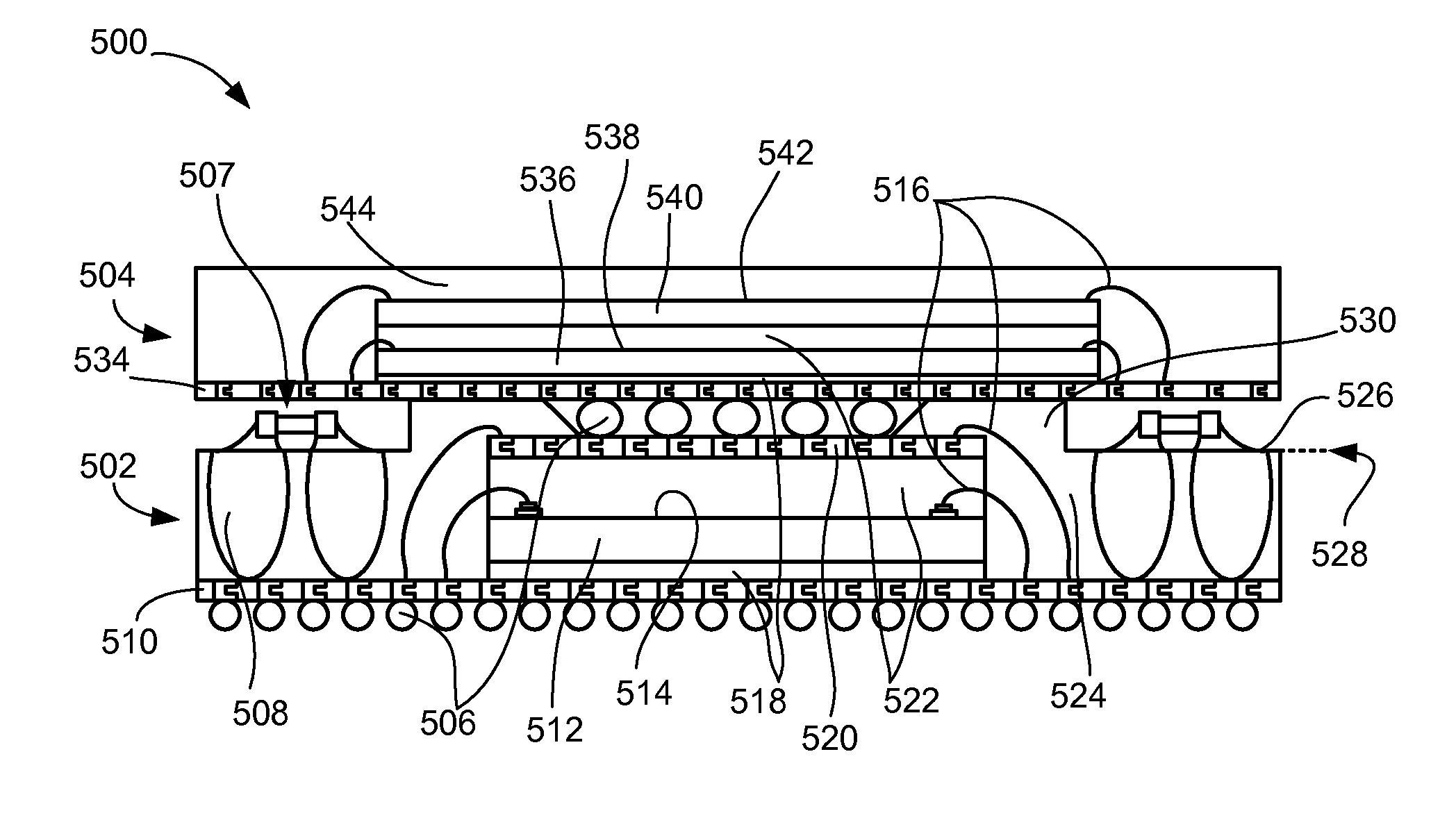
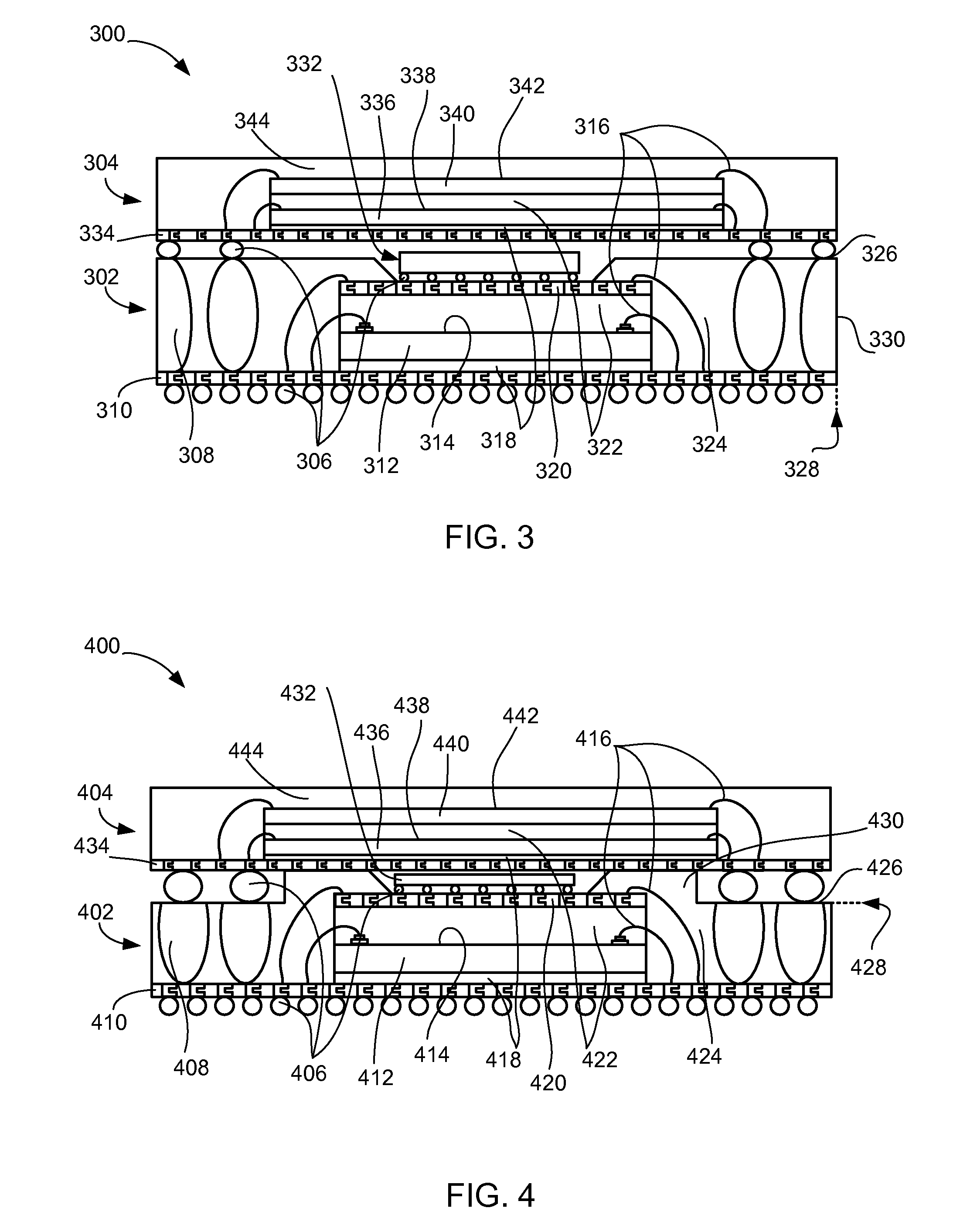
[0046]Referring now to FIG. 3, therein is shown a cross-sectional view of an integrated circuit package system 300 in the present invention. The integrated circuit package system 300 is shown having a first package 302 with a second package 304 mounted above.

[0047]The second package 304 is connected to the first package 302 with interconnections such as solder balls 306. The solder balls 306 connecting the first package 302 to the second package 304 are connected to exposed interconnects 308. The exposed interconnects 308 may be solder balls, conductive pins, or through vias.

[0048]It has been discovered that the use of the exposed interconnects 308 allow for an inexpensive solution to previously difficult and expensive problems of routing signals vertically through package on package systems.

[0049]The exposed interconnects 308 are mounted above a substrate 310 such as a laminated plastic or a ceramic substrate. Also mounted above the substrate 310 is an integrated circuit 312 such a...

third embodiment

[0061]Referring now to FIG. 4, therein is shown a cross-sectional view of an integrated circuit package system 400 in the present invention. The integrated circuit package system 400 is shown having a first package 402 with a second package 404 mounted above.

[0062]The second package 404 is connected to the first package 402 with interconnections such as solder balls 406. The solder balls 406 connecting the first package 402 to the second package 404 are connected to exposed interconnects 408. The exposed interconnects 408 may be solder balls, conductive pins, or through vias.

[0063]It has been discovered that the use of the exposed interconnects 408 allow for an inexpensive solution to previously difficult and expensive problems of routing signals vertically through package on package systems.

[0064]The exposed interconnects 408 are mounted above a substrate 410 such as a laminated plastic or a ceramic substrate. Also mounted above the substrate 410 is an integrated circuit 412 such a...


PUM


Abstract

An integrated circuit package system includes: providing a substrate; mounting an integrated circuit above the substrate; connecting an interposer to the integrated circuit with a wire-in-film adhesive; connecting an exposed interconnect having an upper surface to the substrate; and encapsulating the integrated circuit with an encapsulation.

Description

CROSS-REFERENCE TO RELATED APPLICATION(S)[0001]The present application contains subject matter related to co-pending U.S. patent application Ser. No. 12 / 057,360. The related application is assigned to STATS ChipPAC Ltd.[0002]The present application contains subject matter related to co-pending U.S. patent application Ser. No. 12 / 053,751. The related application is assigned to STATS ChipPAC Ltd.TECHNICAL FIELD[0003]The present invention relates generally to integrated circuits and more particularly to a system for utilizing an exposed interconnect in a package on package system.BACKGROUND ART[0004]The rapidly growing portable electronics market, e.g. cellular phones, laptop computers, and PDAs, are an integral facet of modern life. The multitude of portable devices represents one of the largest potential market opportunities for next generation packaging. These devices have unique attributes that have significant impacts on manufacturing integration, in that they must be generally sm...

Claims


Application Information

Patent Timeline
Patent Type & Authority Patents(United States)
IPC IPC(8): H05K7/00
CPCH01L23/3128H01L25/0657H01L25/105H01L2225/1088H01L24/31H01L24/48H01L2224/16225H01L2224/32225H01L2224/48091H01L2224/48225H01L2224/48227H01L2224/48465H01L2224/73215H01L2224/73265H01L2225/0651H01L2225/06517H01L2225/06586H01L2225/1058H01L2924/14H01L2924/15311H01L2924/15331H01L2924/1815H01L2924/19107H01L24/16H01L2225/1023H01L2225/1041H01L2224/32145H01L2924/10253H01L2924/00014H01L2924/00H01L2924/00012H01L24/73H01L2224/04042H01L2924/00011H01L2924/12042H01L2924/181H01L2224/0401H01L2224/45099H01L2224/45015H01L2924/207
Inventor PAGAILA, REZA ARGENTYDO, BYUNG TAICHUA, LINDA PEI EE
Owner STATS CHIPPAC LTD
Features
  • R&D
  • Intellectual Property
  • Life Sciences
  • Materials
  • Tech Scout
  • Unparalleled Data Quality
  • Higher Quality Content
  • 60% Fewer Hallucinations
Learn More