Printed circuit board

a printed circuit board and circuit board technology, applied in printed circuit aspects, high-frequency circuit adaptations, electrical apparatus construction details, etc., can solve problems such as degrading the performance of pcbs

Active Publication Date: 2012-09-18
CLOUD NETWORK TECH SINGAPORE PTE LTD
View PDF3 Cites 14 Cited by
  • Summary
  • Abstract
  • Description
  • Claims
  • Application Information

AI Technical Summary

Problems solved by technology

However, only portions of the vias are used for transmitting signals, leaving other portions of the vias as stubs which can cause signal reflection thus degrading performance of the PCBs.

Method used


Image

  • Printed circuit board
  • Printed circuit board
  • Printed circuit board

Examples


Embodiment Construction

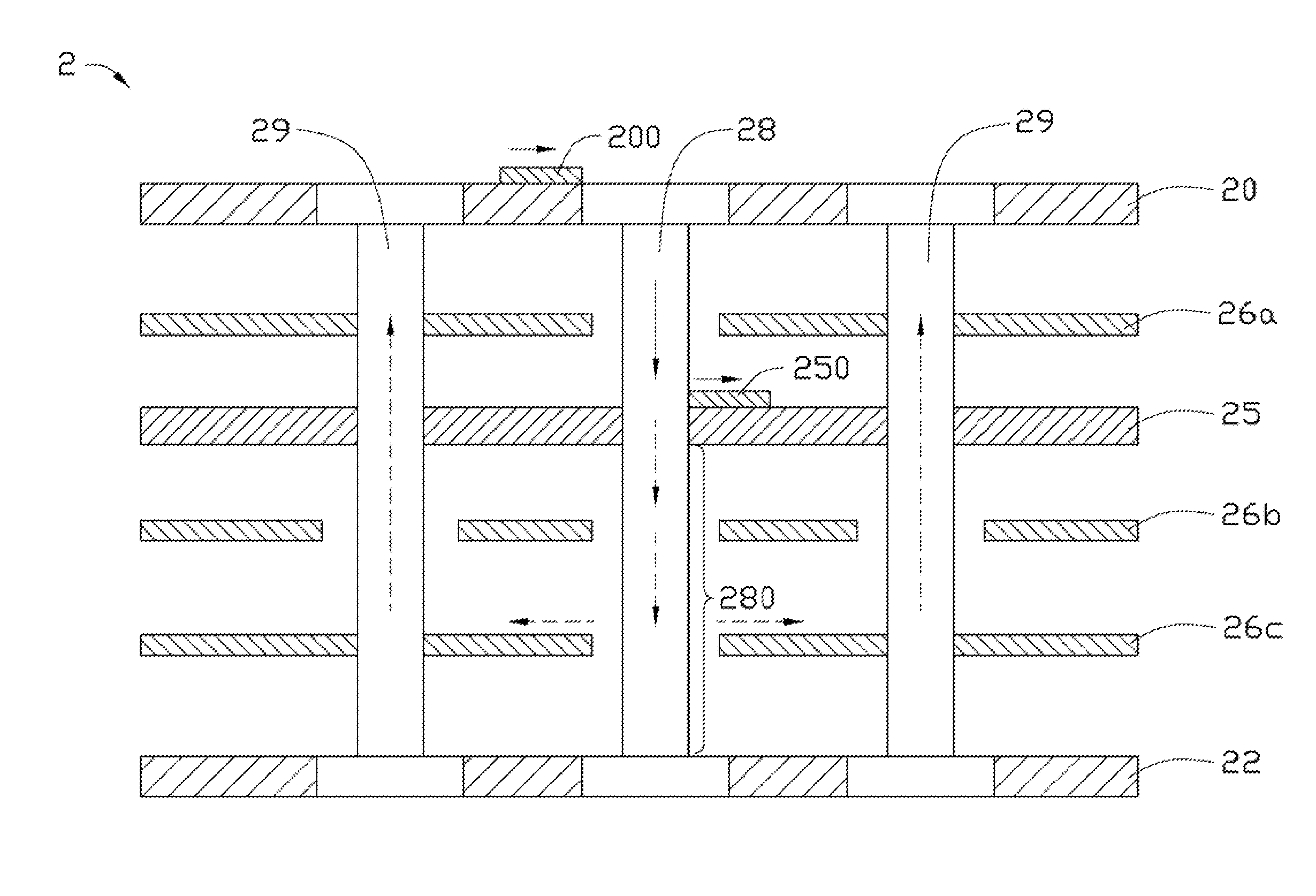
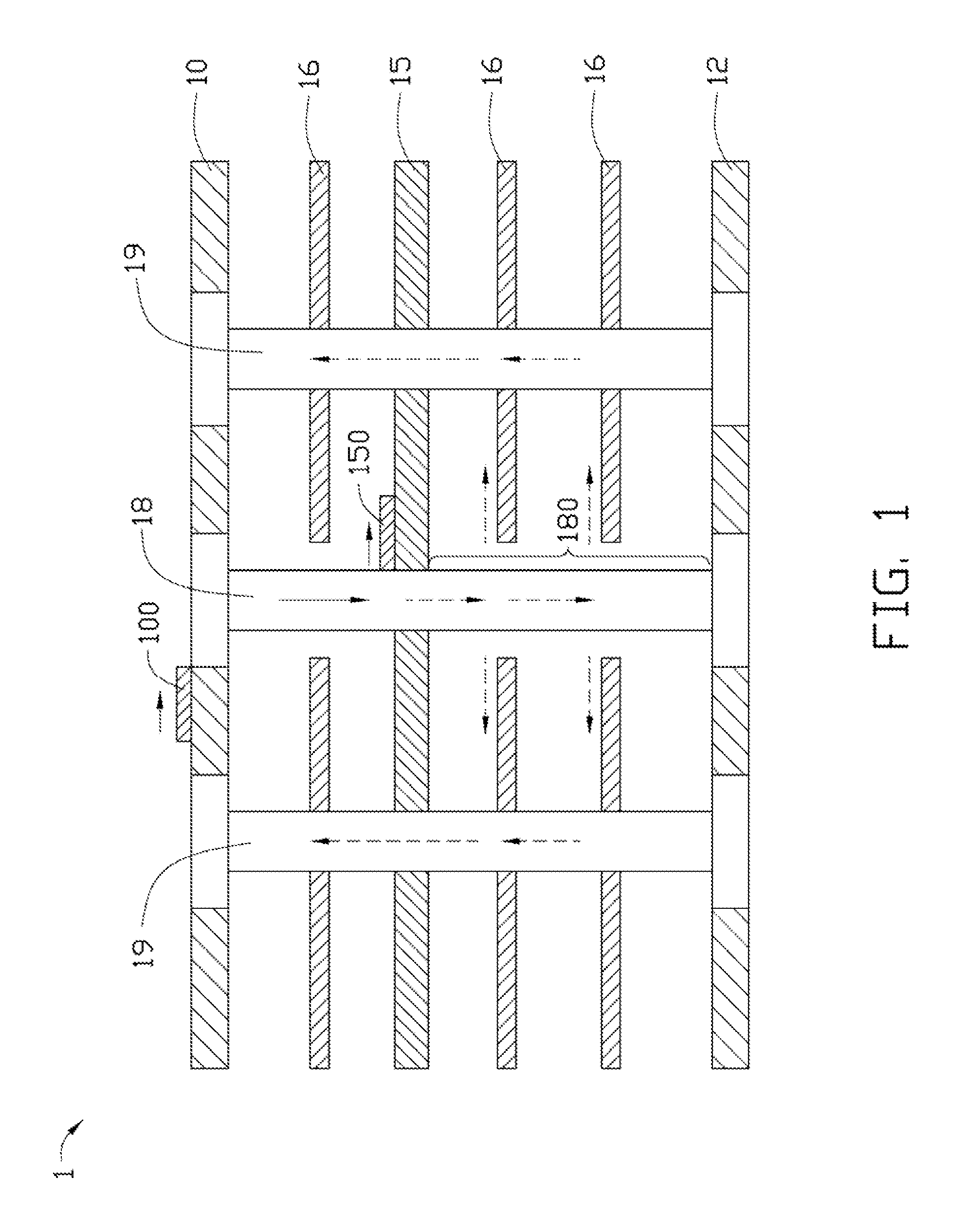
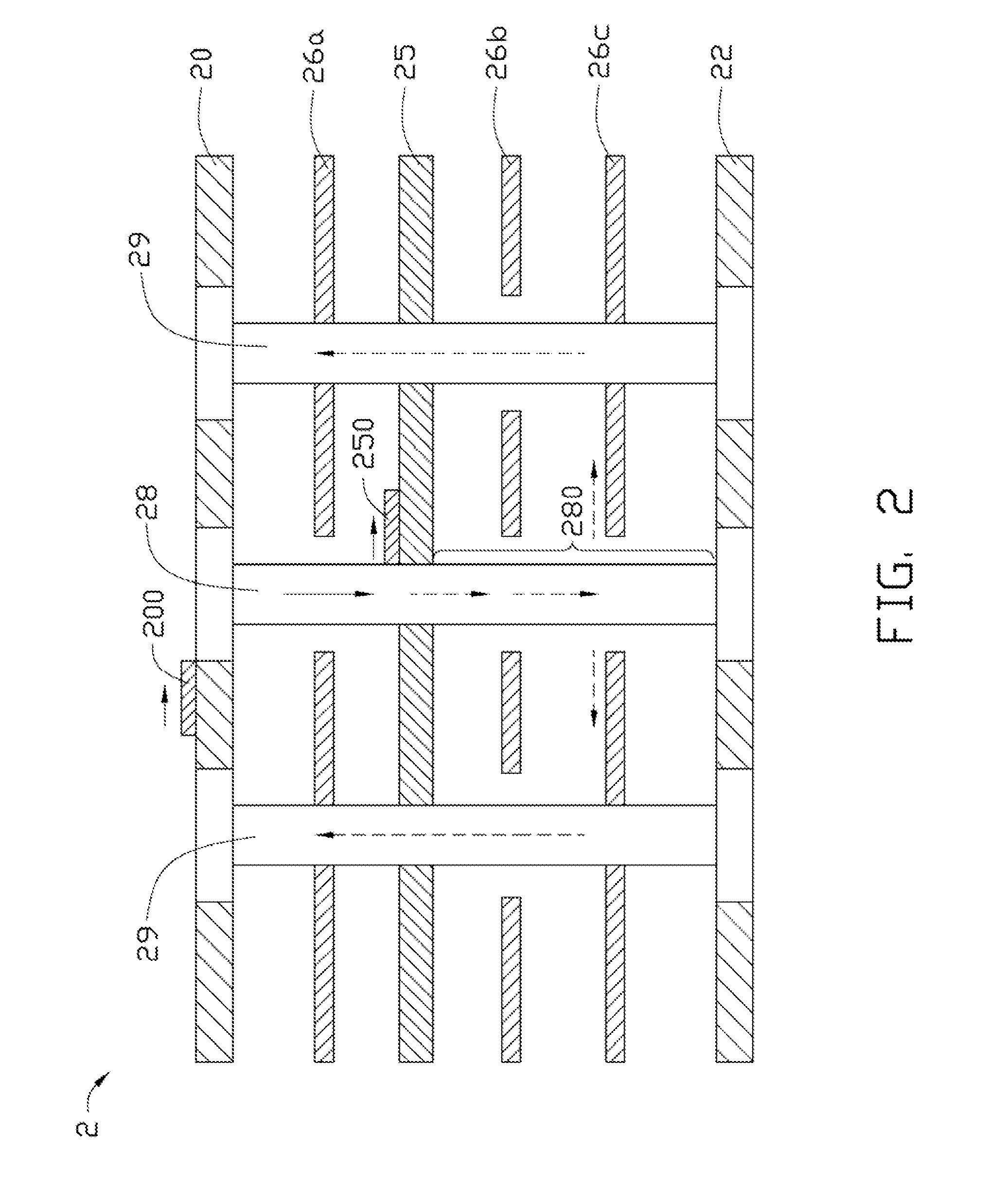
[0009]Referring to FIG. 1, a first exemplary embodiment of a printed circuit board 1 is a multi-layered circuit board such as a high-speed digital circuit board, for forming a high-speed signal transmission circuit on the high-speed digital circuit board. The printed circuit board 1 includes a first signal layer 10, a second signal layer 12, a third signal layer 15, a plurality of ground layers 16, a first via 18, and two second vias 19. A transmission line 100 is located on the first signal layer 10, and a transmission line 150 is located on the third signal layer 15.

[0010]The first signal layer 10 is on the top of the printed circuit board 1. The second signal layer 12 is on the bottom of the printed circuit board 1. The plurality of ground layers 16 are located between the first signal layer 10 and the second signal layer 12. The third signal layer 15 is located between two of the plurality of ground layers 16.

[0011]The first via 18 passes through the printed circuit board 1, and...


PUM


Abstract

A printed circuit board includes a number of signal layers, a number of ground layers, a first transmission line, a second transmission line, a first via, and a second via. The first transmission is located on one of the number of signal layers. The second transmission line is located on another of the number of signal layers. The first and second vias pass through the printed circuit board. The first via is electrically coupled to the first and second transmission lines, and is isolated from the number of ground layers. The second via is electrically coupled to one or more of the number of ground layers, and is isolated from the other of the number of ground layers to increase an inductance, thus compensating capacitive nature of an open stub and improving signal integrity.

Description

BACKGROUND[0001]1. Technical Field[0002]The present disclosure relates to printed circuit boards.[0003]2. Description of Related Art[0004]Multilayer printed circuit boards (PCBs) are commonly used in electronic devices to connect electronic components such as integrated circuits to one another. Signals between different layers are transmitted through vias connecting transmission lines across different layers. However, only portions of the vias are used for transmitting signals, leaving other portions of the vias as stubs which can cause signal reflection thus degrading performance of the PCBs.BRIEF DESCRIPTION OF THE DRAWINGS[0005]FIG. 1 is a schematic diagram of a first exemplary embodiment of a printed circuit board.[0006]FIG. 2 is a schematic diagram of a second exemplary embodiment of a printed circuit board.[0007]FIG. 3 is a schematic diagram of a third exemplary embodiment of a printed circuit board.[0008]FIG. 4 is a simulation graph of insertion loss for the printed circuit b...

Claims


Application Information

Patent Timeline
Patent Type & Authority Patents(United States)
IPC IPC(8): H05K1/11H05K7/00H05K1/14
CPCH05K1/0251H05K1/0222H05K3/429H05K2201/09309H05K2201/09636
Inventor LIU, CHIEN-HUNGHSU, SHOU-KUOPAI, YU-CHANGHSIEH, PO-CHUAN
Owner CLOUD NETWORK TECH SINGAPORE PTE LTD
Why Eureka
Try Eureka