
Trench MOSFET having shielded electrode integrated with trench Schottky rectifier

a technology of trench mosfet and trench mosfet, which is applied in the field of cell structure and device configuration of semiconductor devices, can solve problems such as reducing the efficiency of trench mosfet, and achieve the effect of improving operation performan

Active Publication Date: 2012-09-25
FORCE MOS TECH CO LTD
View PDF4 Cites 23 Cited by
  • Summary
  • Abstract
  • Description
  • Claims
  • Application Information

AI Technical Summary

Benefits of technology

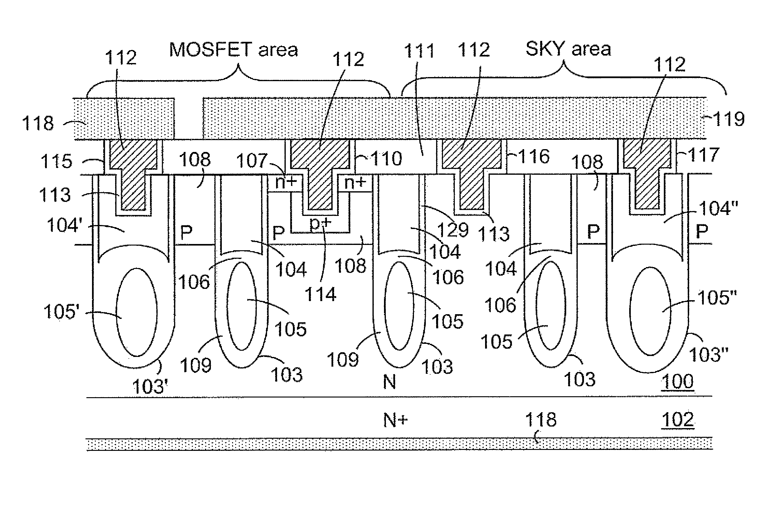
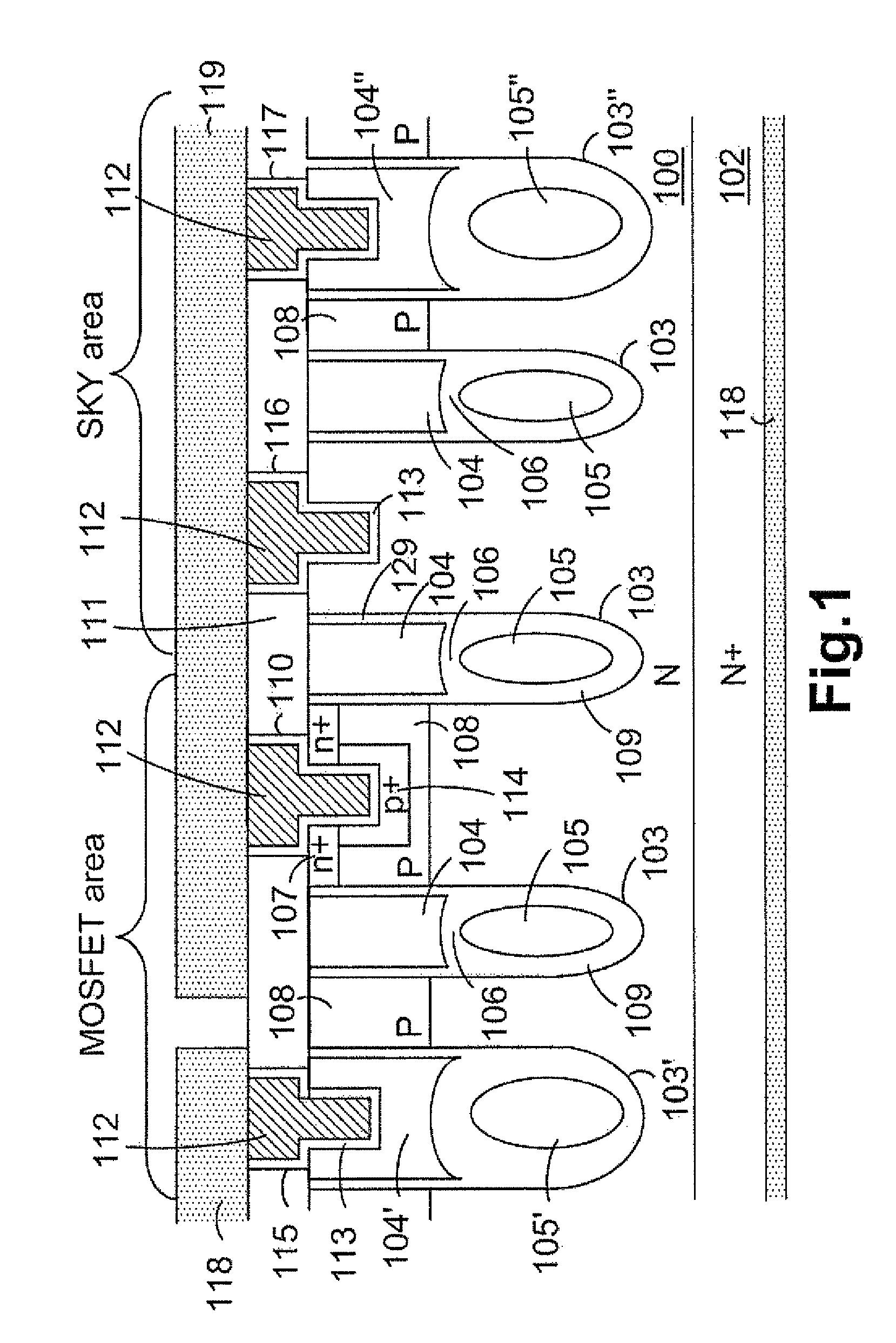
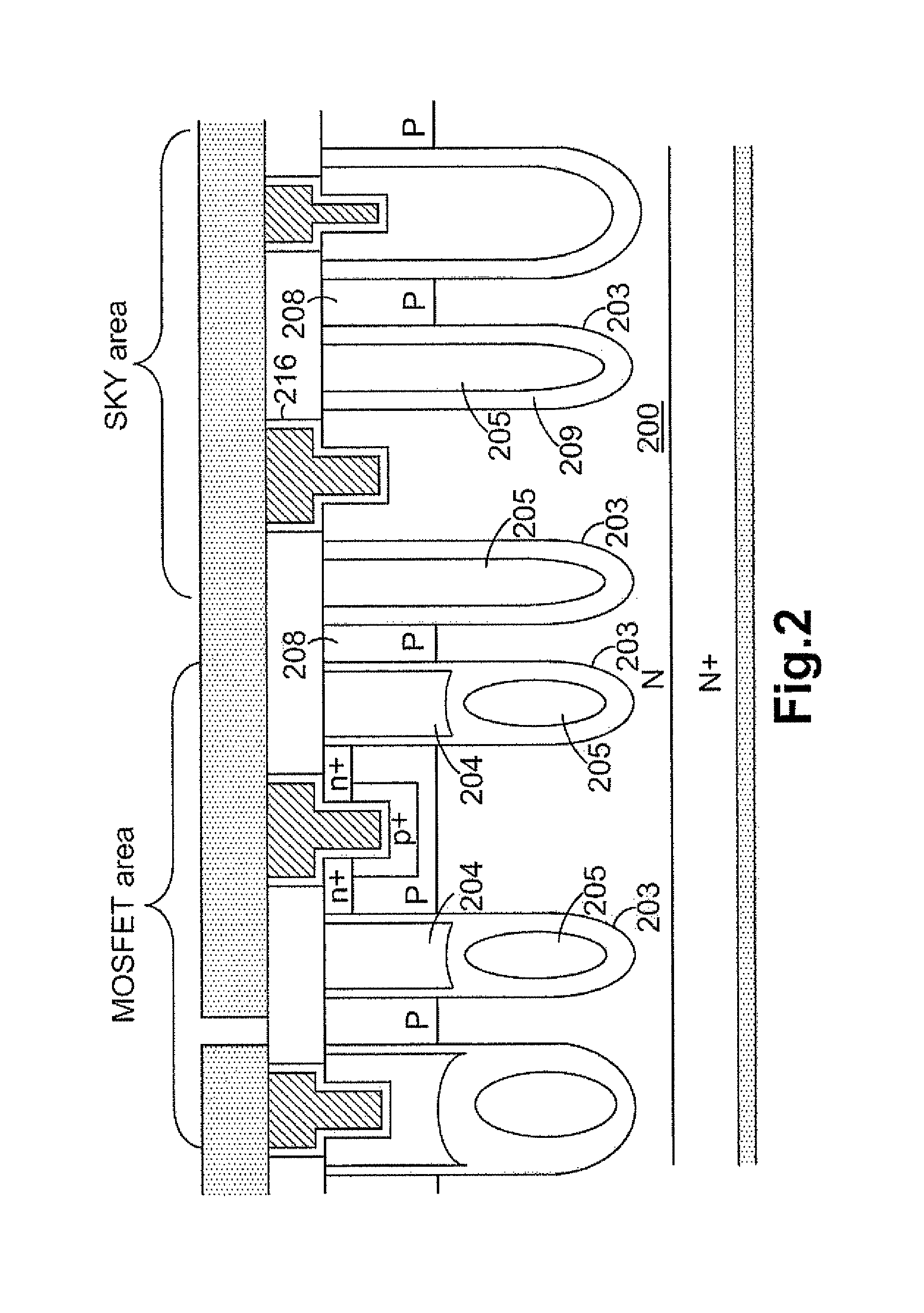
[0005]It is therefore an object of the present invention to provide a new and improved semiconductor power device such as an integrated circuit comprising a trench MOSFET having shielded electrode and a trench Schottky rectifier on a single chip for better operation performance. According to the present invention, there is provided an integrated circuit comprising a plurality of trench MOSFETs and a plurality of trench Schottky rectifiers horizontally disposed in two different areas further comprising: a substrate of a first conductivity type; an epitaxial layer of the first conductivity type over the substrate, the epitaxial layer having a lower doping concentration than the substrate; a plurality of gate trenches extending into the epitaxial layer; a trench MOSFET comprising a gate electrode over a shielded electrode in each the gate trench wherein the gate electrode and the shielded electrode insulated from each other by an inter-electrode insulation layer, and the gate electrode is insulated from a source region of the first conductivity type and body region of a second conductivity type by a first gate insulation layer and the shield electrode is insulated from the epitaxial layer by a second gate insulation layer; the first gate insulation layer along the gate trenches is less than the second insulation layer; the gate electrode surrounded by the source region encompassed in the body region above the shielded electrode; the gate electrode connected to a gate metal and the shielded electrode to a source metal; a contact insulation layer covering the integrated circuit with a source-body contact trench opened in the trench MOSFET through the source and extended into the body regions and filled with a contact metal plug overlying a barrier metal layer therein, the contact metal plug filled in the source-body contact trench connected with the source metal; a trench Schottky rectifier formed into the epitaxial layer in a different area from the trench MOSFET and having a Schottky barrier layer lined in a Schottky contact trench filled with the contact metal plug overlying the barrier metal layer directly contacting the Schottky contact trench bottom and sidewalls, and between a pair of adjacent gate trenches wherein the source and body regions do not exist, the contact metal plug filled in the Schottky contact trench connected with an anode metal; the gate trenches in the trench MOSFET and trench Schottky rectifier having a greater trench depth than the Schottky contact trench into the epitaxial layer; the Schottky rectifier formed at least along sidewalls of the Schottky contact trench in the epitaxial layer, separated from the pair of adjacent gate trenches by the epitaxial layer without having the source and body regions surrounding the Schottky contact trench sidewalls; at least a gate contact trench in the trench MOSFET opened through the contact insulation layer and extended into the gate electrode in a wide gate trench having a greater trench width than the gate trenches in the trench MOSFET, and filled with the contact metal plug overlying a barrier metal layer therein, the contact metal plug filled in the gate contact trench connected with the gate metal; and the source metal and the anode metal connected together as a source / anode metal.

Problems solved by technology

Meanwhile, in order to further increase the efficiency of the trench MOSFET having shielded electrode, the parasitic PN body diode of the trench MOSFET must be prevented from turning on, because once the parasitic PN body diode is turned on, both electron and hole carriers are generated that requires longer time to eliminate these carriers through the electron-hole combinations, thus reducing the efficiency of the trench MOSFET.

Method used


Image

  • Trench MOSFET having shielded electrode integrated with trench Schottky rectifier
  • Trench MOSFET having shielded electrode integrated with trench Schottky rectifier
  • Trench MOSFET having shielded electrode integrated with trench Schottky rectifier

Examples


Embodiment Construction

[0016]Please refer to FIG. 1 for a preferred N-channel integrated circuit comprising a trench MOSFET and a trench Schottky rectifier (SKY, as illustrated in FIG. 1) on a single chip. The N-channel circuit is formed in an N epitaxial layer 100 supported on a heavily doped N+ substrate 102 which coated with back metal 118 on the rear side as drain / cathode metal. A plurality of gate trenches 103 are formed extending in the N epitaxial layer 100, each of the gate trenches 103 is filled with a gate electrode 104 over a shielded electrode 105, wherein the gate electrode 104 and the shielded electrode 105 is insulated from each other by an inter-electrode insulation layer 106, the gate electrode 104 is insulated from an N+ source region 107 and a P body region 108 by a first gate oxide layer 129 and the shielded electrode 105 is insulated from the epitaxial layer 100 by a second gate insulation layer 109, wherein the gate electrode 104 is surrounded by the N+ source region 107 encompassed ...


PUM


Abstract

A trench MOSFET having shielded gate in parallel with trench Schottky rectifier is formed on a single chip to further increase the efficiency of the trench MOSFET having shielded electrode. As the size of present device is getting smaller and smaller, the trench Schottky rectifier of this invention is able to be shrink and, at the same time, to achieve lower forward voltage drop and lower reverse leakage current.

Description

CROSS-REFERENCES TO RELATED APPLICATIONS[0001]This application claims priority from application Ser. No. 12 / 659,639 filed Mar. 16, 2010 which is continuation in part of application Ser. No. 12 / 213,628 now U.S. Pat. No. 7,816,732.FIELD OF THE INVENTION[0002]This invention relates generally to the cell structure, device configuration of semiconductor devices. More particularly, this invention relates to an improved trench MOSFET (Metal Oxide Semiconductor Field Effect Transistor) having shielded electrode integrated with trench Schottky rectifier on a single chip to improve operation efficiency.BACKGROUND OF THE INVENTION[0003]Trench MOSFET having gate electrode over shielded electrode structure provides advantages over conventional trench MOSFET, such as reduced gate to drain charge Qgd, and reduced on-resistance. See for example, U.S. Pat. Nos. 5,998,833 and 7,768,064. The superior performance of the trench MOSFET having shielded electrode is an excellent choice for DC / DC converter....

Claims


Application Information

Patent Timeline
Patent Type & Authority Patents(United States)
IPC IPC(8): H01L29/78
CPCH01L29/407H01L29/41766H01L29/42372H01L29/7806H01L29/7813H01L29/8725H01L29/0878H01L29/42368H01L29/47
Inventor HSIEH, FU-YUAN
Owner FORCE MOS TECH CO LTD
Learn More