Method and system for intra-printed circuit board communication via waveguides

a technology of printed circuit board and waveguide, which is applied in the field of wireless communication, can solve the problems of power inefficiency of transmitters and/or receivers in comparison to other blocks of portable communication devices

Active Publication Date: 2012-09-25
AVAGO TECH INT SALES PTE LTD
View PDF18 Cites 14 Cited by
  • Summary
  • Abstract
  • Description
  • Claims
  • Application Information

AI Technical Summary

Problems solved by technology

Additionally, transmit and / or receive circuitry within such mobile wireless devices often account for a significant portion of the power consumed within these devices.
Moreover, in some conventional communication systems, transmitters and / or receivers are often power inefficient in comparison to other blocks of the portable communication devices.

Method used


Image

  • Method and system for intra-printed circuit board communication via waveguides
  • Method and system for intra-printed circuit board communication via waveguides
  • Method and system for intra-printed circuit board communication via waveguides

Examples


Embodiment Construction

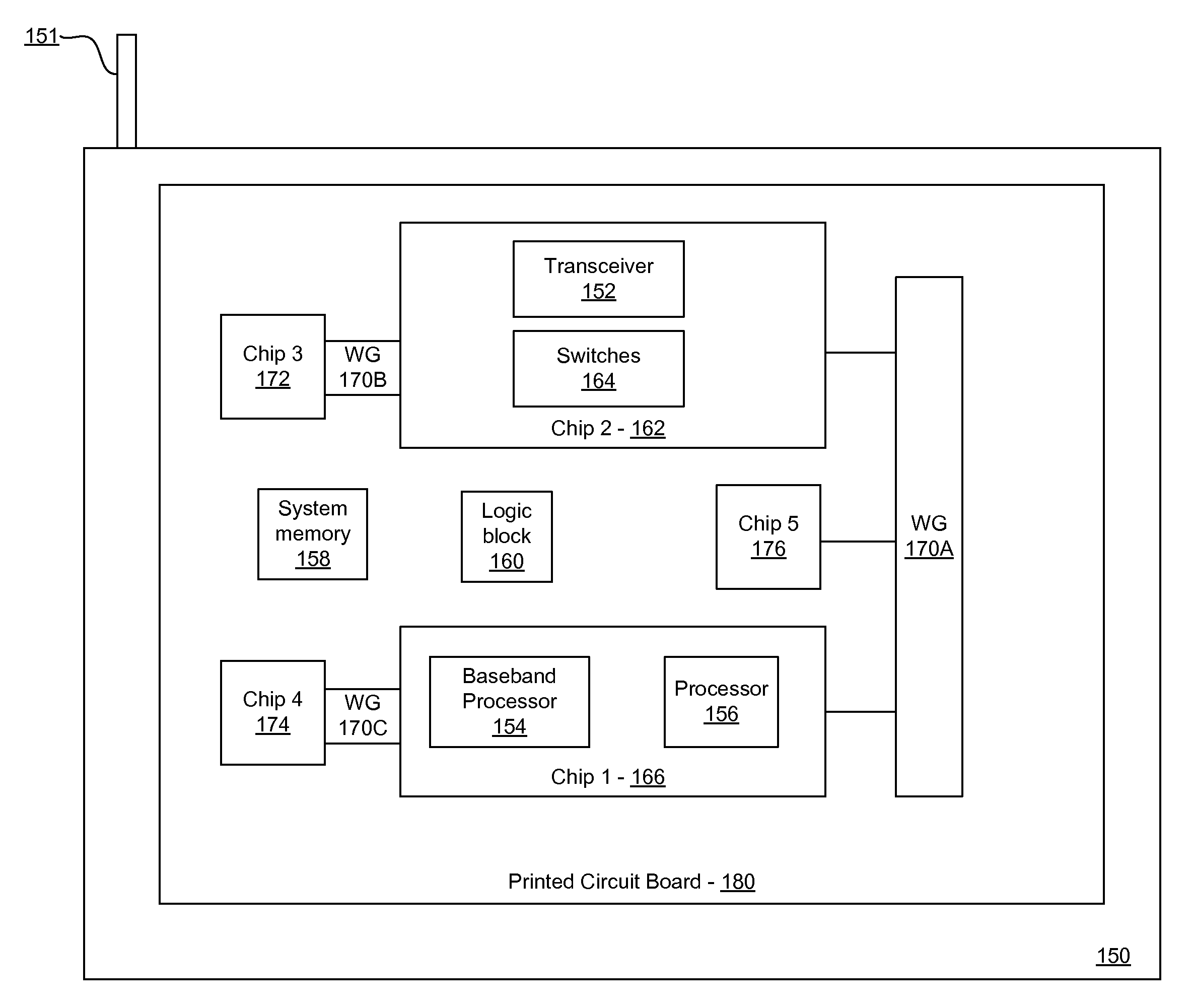
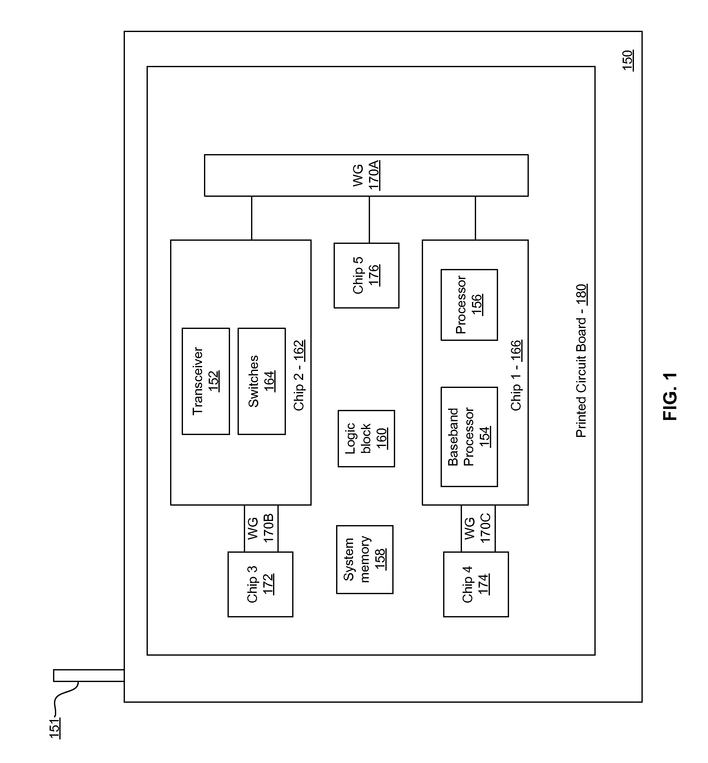
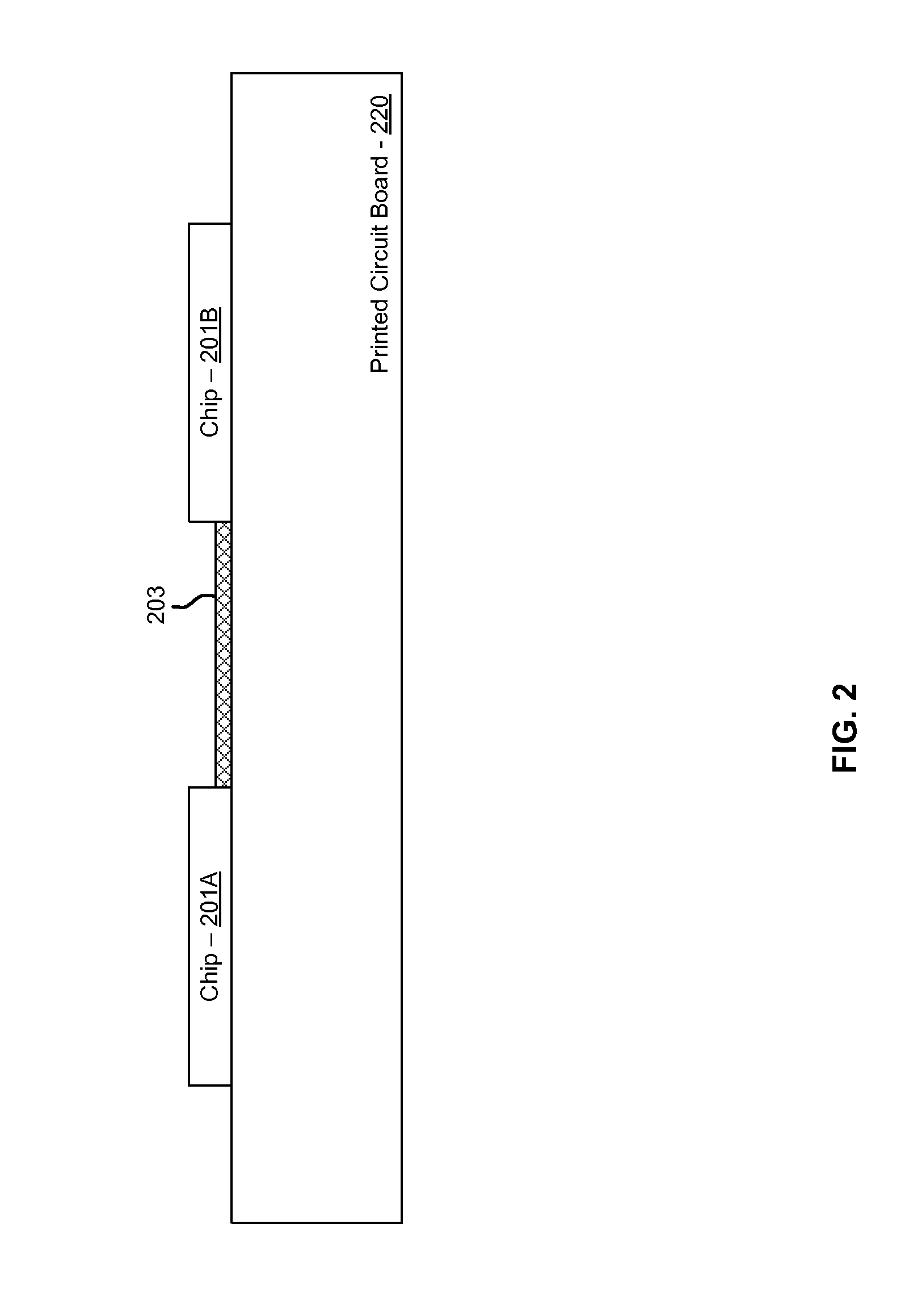
[0019]Certain aspects of the invention may be found in a method and system for intra-printed circuit board communication via waveguides. Exemplary aspects of the invention may comprise communicating one or more signals between or among a plurality of integrated circuits via one or more waveguides integrated on a printed circuit board. The integrated circuits may be bonded to the printed circuit board. The waveguides may be configured via switches integrated within each of the plurality of integrated circuits. The signals communicated via the waveguides may comprise microwave signals. The one or more waveguides may be configured for communicating microwave signals with a frequency of 60 GHz or greater. The communication of the one or more signals may be configured via a low frequency control signal, which may comprise a digital signal. The one or more waveguides may comprise metal and / or semiconductor layers deposited on and / or embedded within the printed circuit board.

[0020]FIG. 1 i...


PUM


Abstract

Methods and systems for intra-printed circuit board communication via waveguides are disclosed and may include communicating one or more signals between or among a plurality of integrated circuits via one or more waveguides integrated on a printed circuit board. The integrated circuits may be bonded to the printed circuit board. The waveguides may be configured via switches integrated within each of the plurality of integrated circuits. The one or more signals may include microwave signals. The one or more waveguides may be configured for communicating microwave signals with a frequency of 60 GHz or greater. The communication of the one or more signals may be configured via a low frequency control signal, which may include a digital signal. The one or more waveguides may include metal and / or semiconductor layers deposited on and / or embedded within the printed circuit board.

Description

CROSS-REFERENCE TO RELATED APPLICATIONS / INCORPORATION BY REFERENCE[0001]This application makes reference to and claims priority to U.S. Provisional Application Ser. No. 61 / 073,934 filed on Jun. 19, 2008, which is hereby incorporated herein by reference in its entirety.[0002]This application makes also reference to:[0003]U.S. patent application Ser. No. 12 / 191,553 filed on Aug. 14, 2008;[0004]U.S. patent application Ser. No. 12 / 058,423 filed on Mar. 28, 2008; and[0005]U.S. patent application Ser. No. 12 / 191,605 filed on Aug. 14, 2008.[0006]Each of the above stated applications is hereby incorporated herein by reference in its entirety.FEDERALLY SPONSORED RESEARCH OR DEVELOPMENT[0007][Not Applicable]MICROFICHE / COPYRIGHT REFERENCE[0008][Not Applicable]FIELD OF THE INVENTION[0009]Certain embodiments of the invention relate to wireless communication. More specifically, certain embodiments of the invention relate to a method and system for intra-printed circuit board communication via wav...

Claims


Application Information

Patent Timeline
Patent Type & Authority Patents(United States)
IPC IPC(8): H01L23/58
CPCH05K1/0237H05K1/181H05K2201/10674
Inventor ROFOUGARAN, AHMADREZAROFOUGARAN, MARYAM
Owner AVAGO TECH INT SALES PTE LTD
Why Eureka
Try Eureka