Printed electronics

a technology of printed electronics and printed circuits, applied in resistive material coatings, polyether coatings, inks, etc., can solve the problems of limited substrates, insufficient electrically conductive printed circuits, and insufficient conductive polymers alon

Active Publication Date: 2012-10-02
VORBECK MATERIALS CORP +1
View PDF21 Cites 56 Cited by
  • Summary
  • Abstract
  • Description
  • Claims
  • Application Information

AI Technical Summary

Problems solved by technology

However, conductive polymers alone are generally not sufficiently electrically conductive.
Furthermore, the resulting printed metallic circuits are usually insufficiently electrically conductive to be effective in most applications, including in devices in which the circuits are regularly stressed by bending and / or stretching during use.
The temperatures used in sintering processes frequently limit the substrates that can be selected for the preparation of the electronics.
For example, while it would be desirable to use inexpensive materials such as paper, polyolefins (e.g., polypropylene), and the like as substrates for printed electronics in many applications, the sintering temperatures often required are too high to be used with paper.
Furthermore, silver is costly and other, non-precious, metals can form oxides upon exposure to the environment that can render the material insufficiently conductive for the application.
Additionally, the use of metal-based inks can add weight to the resulting device, and the aforementioned sintering process can add one or more additional steps, time, and complexity to the fabrication process.

Method used


Image

  • Printed electronics
  • Printed electronics

Examples


example 1

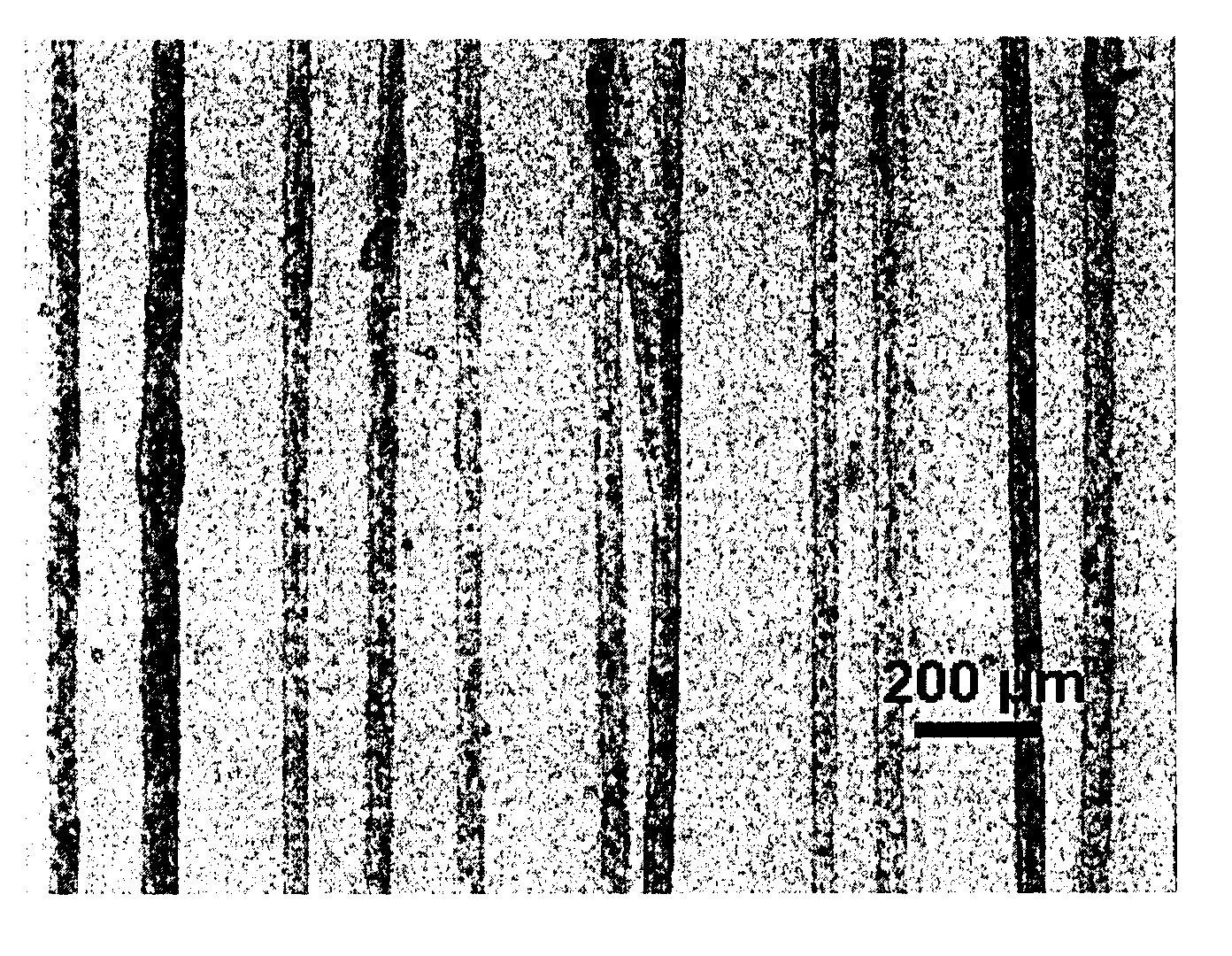
[0056]An ink is prepared as described above using PEO having a molecular weight of 4,000,000. The ink is printed electrohydrodynamically onto a glass substrate using the method disclosed in WO 2007 / 053621. The printing is done at a flow rate of 0.5 mL / hr under a 2200 kV potential difference between electrodes that are 7.2 mm apart. The width of the lines is about 43 μm. FIG. 1 is an optical microscope image of a series of parallel printed lines.

[0057]Copper tapes are attached to the lines perpendicular to the length of the lines. A power supply (Tektronix PS 252G Programmable Power Supply, Tektronix Inc., Beaverton, Oreg.) and a multimeter (Fluke 27 Multimeter, Fluke Corp., Everett, Wash.) are attached in serial with the printed via the copper tapes. A potential difference (5-20 V) is applied and current is monitored through the multimeter. An electrometer (Keithley 6514, Keithley Instruments Inc., Cleveland, Ohio) with two electrodes is used to measure the potential difference acro...

example 2

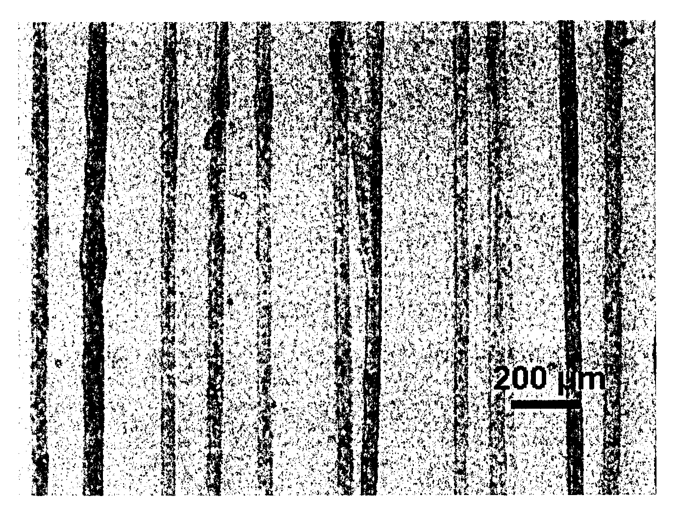
[0058]An ink is prepared as described above using PEO having a molecular weight of 4,000,000. The ink is printed electrohydrodynamically onto a glass substrate using the method disclosed in WO 2007 / 053621. The printing is done at a flow rate of 0.5 mL / hr under a 2200 kV potential difference between electrodes that are 7.2 mm apart. The width of the lines is about 130 μm.

[0059]The ink is formed into a film as follows: two copper plates (22 mm×22 mm) are wrapped with Teflon tape, leaving 1 mm of copper uncovered at the lower ends. The plates are then firmly attached to the shorter of the side walls of a Teflon® cell (23 mm×46 mm inner base area, 32 mm height) with screws. The mixture is poured into the Teflon® cell and kept at 50° C. on a hot plate until all of the solvent is evaporated to form films that are attached to the copper plates.

[0060]Copper tapes are attached parallel to each other on two ends of the film such that they cover the entire width of the film. The electrical con...

example 3

[0063]An ink is prepared as described above using PEO having a molecular weight of 4,000,000. The ink is printed electrohydrodynamically onto a glass substrate using the method disclosed in WO 2007 / 053621. The printing is done at a flow rate of 0.5 mL / hr under a 2200 kV potential difference between electrodes that are 7.2 mm apart. The width of the lines is about 140 μm and the thickness is about 300 nm. The printed line has an electrical conductivity of about 19.6 S / m.

General Details for Examples 4-14

Preparation of Test Samples

[0064]The inks in the form of liquid dispersions are printed onto a substrate using a doctor blade and then dried in air in an oven at 125° C. to form a film. Testing is done on the printed films.

Electrical Conductivity

[0065]The point-to-point resistivity (in ohms) of the films is measured using a standard multimeter across contact points consisting of two spots of silver paste having a diameter of about 0.3 mm that are applied to the surface of the film abou...


PUM

PropertyMeasurementUnit
temperaturesaaaaaaaaaa
surface areaaaaaaaaaaa

Abstract

Printed electronic device comprising a substrate onto at least one surface of which has been applied a layer of an electrically conductive ink comprising functionalized graphene sheets and at least one binder. A method of preparing printed electronic devices is further disclosed.

Description

[0001]This invention was made with Government support under Grant No. CMS-0609049, awarded by the National Science Foundation, and under Grant No. NCC1-02037, awarded by NASA. The Government has certain rights in the invention.FIELD OF THE INVENTION[0002]The present invention relates to printed electronic devices and methods for their manufacture.BACKGROUND[0003]Printed electronics are increasingly finding uses in a great variety of applications, including portable electronics, signage, lighting, product identification, packaging flexible electronic devices (such as those that can be rolled or bent), photovoltaic devices, medical and diagnostic devices, antennas (including RFID antennas), displays, sensors, thin-film batteries, electrodes and myriad others. Printed electronics have a variety of advantages over electronics made using other methods, including subtractive methods. Printing can be faster than normal subtractive methods (such as etching) and can generate less waste and i...

Claims


Application Information

Patent Timeline
Patent Type & Authority Patents(United States)
IPC IPC(8): H01L23/48H05K1/09C09D7/62C09D7/65
CPCC09C1/46C09D7/125C09D7/1291C09D11/52H05K1/095H05K1/092H05K3/0091C01P2004/02C01P2006/12C08K3/04H01L2924/0002H05K2201/0323H01L2924/00H05K3/10C09D7/65C09D7/70Y10S977/734Y10S977/847Y10S977/932C09D7/62H05K3/12B82Y30/00B82Y40/00C01P2006/40C09D11/037C09D11/102C09D171/02C09D177/00
Inventor CRAIN, JOHN M.LETTOW, JOHN S.AKSAY, ILHAN A.KORKUT, SIBEL A.CHIANG, KATHERINE S.CHEN, CHUAN-HUAPRUD'HOMME, ROBERT K.
Owner VORBECK MATERIALS CORP
Why Eureka
Try Eureka