
Liquid crystal display device having storage lines overlapping active layers formed of polysilicon material

a polysilicon material and active layer technology, applied in non-linear optics, instruments, optics, etc., can solve problems such as reducing aperture ratios, and achieve the effects of enhancing the response speed enhancing the electric charge mobility of an lcd device, and improving the aperture ratio

Active Publication Date: 2012-10-02
LG DISPLAY CO LTD
View PDF11 Cites 2 Cited by
  • Summary
  • Abstract
  • Description
  • Claims
  • Application Information

AI Technical Summary

Benefits of technology

The present invention provides a thin film transistor substrate of poly-silicon type and a fabricating method thereof that improves the aperture ratio without deteriorating the capacitance value of a storage capacitor. The invention also enhances electric charge mobility and response speed of an LCD device. The substrate includes a plurality of gate lines and data lines, a pixel electrode, a thin film transistor, and at least two storage lines positioned on different sides of the pixel electrode. The fabricating method includes forming multiple layers on a substrate, adding a protective film, and forming a pixel electrode. The technical effects of the invention include improved aperture ratio, enhanced electric charge mobility, and improved response speed of an LCD device.

Problems solved by technology

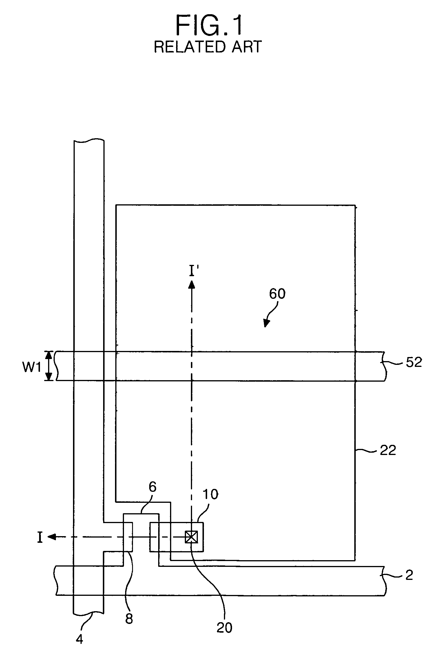
A problem occurs in that the aperture ratio is reduced by an area of the pixel electrode covered by the storage line 52.

Method used


Image

  • Liquid crystal display device having storage lines overlapping active layers formed of polysilicon material
  • Liquid crystal display device having storage lines overlapping active layers formed of polysilicon material
  • Liquid crystal display device having storage lines overlapping active layers formed of polysilicon material

Examples


first embodiment

[0028]FIG. 3 is a plan view showing a portion of a thin film transistor type substrate employing poly-silicon according to the present invention. FIG. 4 are cross-sectional views of the thin film transistor substrate taken along line II-II′ and line III-III′ in FIG. 3. Referring to FIG. 3 and FIG. 4, the thin film transistor (TFT) substrate of poly-silicon type includes a TFT 130 connected to a gate line 102 and a data line 104, and a pixel electrode 122 and a storage capacitor 160 connected to the TFT 130. The TFT 130 is formed as either an N-type or a P-type. Hereinafter, the case of forming the TFT 130 in an N-type will be described.

[0029]The TFT 130 charges a video signal onto the pixel electrode. To this end, the TFT 130 includes a gate electrode 106 connected to the gate line 102, a source electrode 108 connected to the data line 104, a drain electrode 110 connected via a pixel contact hole 120 passing through a protective film 118 to the pixel electrode 122, and a first activ...

second embodiment

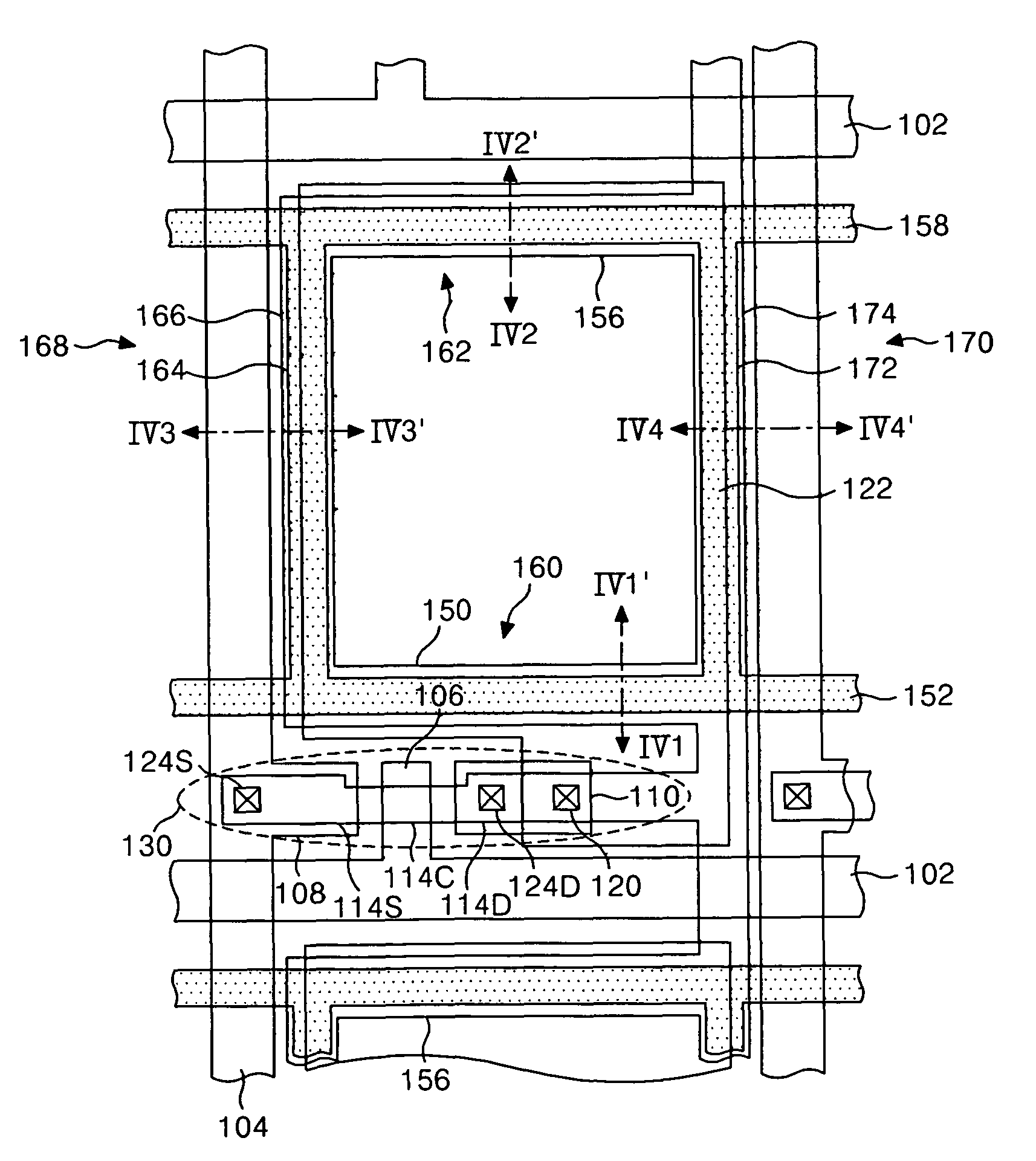
[0034]FIG. 5 is a plan view showing a portion of a thin film transistor type substrate employing poly-silicon according to the present invention. FIG. 6 is a cross-sectional view of the thin film transistor substrate taken along line IV1-IV1′, line IV2-IV2′ and line IV3-IV3′ in FIG. 5. The poly-silicon type TFT substrate shown in FIG. 5 and FIG. 6 has some of the same elements as the poly-silicon type TFT substrate shown in FIG. 3 and FIG. 4 except that third and fourth storage capacitors 168 and 170 extending along the data lines 104 are further provided.

[0035]Storage capacitors 160, 162, 168 and 170 allow video signals charged on the pixel electrode 122 to be stably maintained. To this end, first and second storage capacitors 160 and 162 are positioned adjacent to the gate lines 102 at opposite sides of the pixel electrode 122, and third and fourth storage capacitors 168 and 170 are positioned adjacent to the data lines 104 at opposite sides of the pixel electrode 122.

[0036]The fi...


PUM

PropertyMeasurementUnit
areaaaaaaaaaaa
capacitanceaaaaaaaaaa
light transmittanceaaaaaaaaaa

Abstract

A poly-silicon type thin film transistor substrate includes: a plurality of gate lines and data lines defining a pixel; a pixel electrode in the pixel; a thin film transistor having a gate electrode connected to one of the gate lines, a source electrode connected to one of the data lines, a drain electrode connected to the pixel electrode, and a first active layer of poly-silicon defining a channel between the source electrode and the drain electrode; and at least two storage lines positioned on different sides of the pixel electrode.

Description

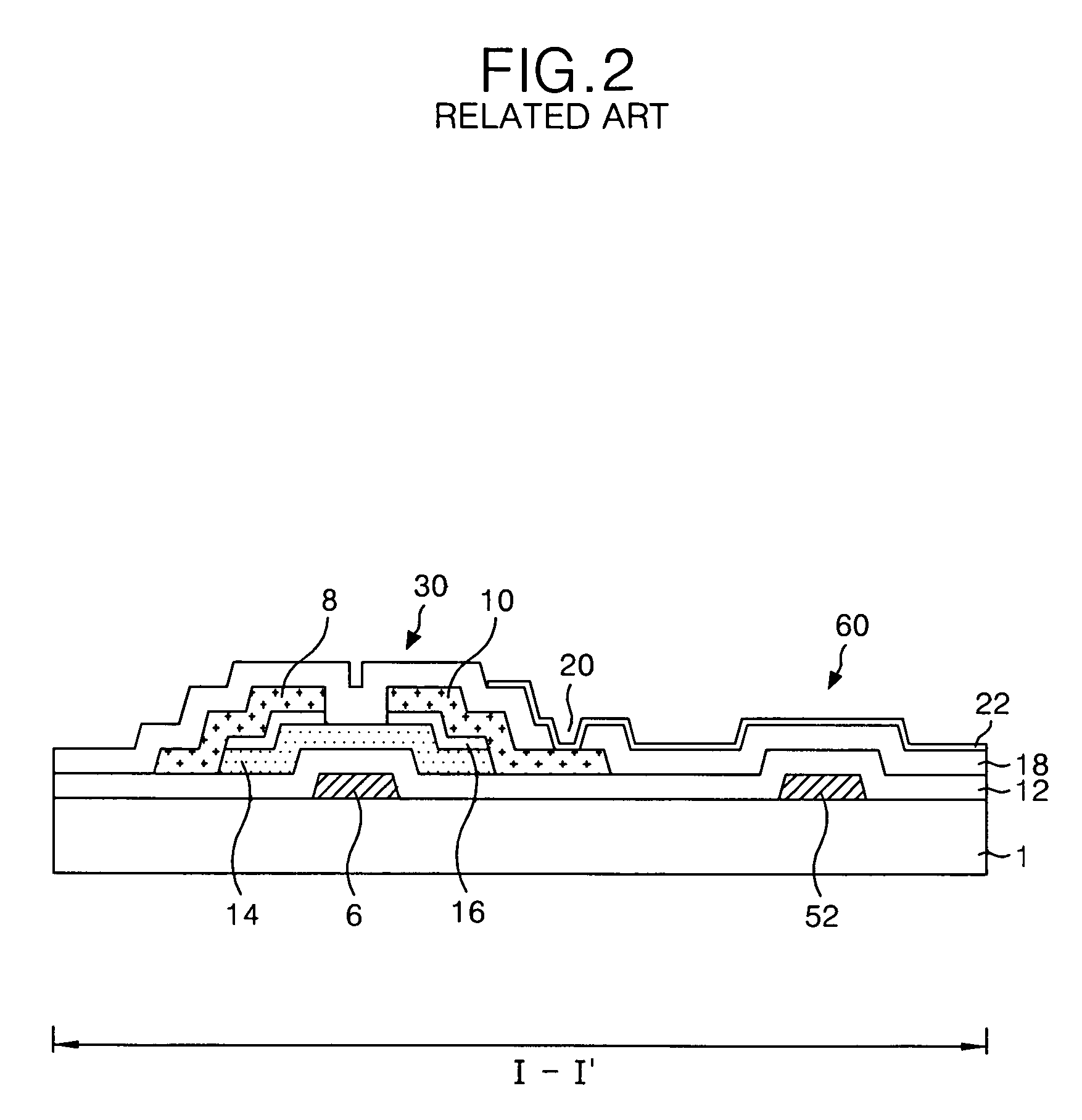
[0001]This application claims the benefit of the Korean Patent Application No. P2004-089400 filed on Nov. 4, 2004, which is hereby incorporated by reference.BACKGROUND OF THE INVENTION[0002]1. Field of the Invention[0003]This invention relates to a liquid crystal display, and more particularly to a thin film transistor substrate of polycrystalline silicon (poly-silicon) type and a fabricating method thereof. Although the present invention is suitable for a wide scope of applications, it is particularly suitable for improving an aperture ratio without a deterioration in a capacitance value of a storage capacitor.[0004]2. Description of the Related Art[0005]Generally, a liquid crystal display (LCD) has liquid crystal cells arranged in a matrix on a liquid crystal display panel to control light transmittance in accordance with video signals so as to display a picture. FIG. 1 is a plan view illustrating a related art thin film transistor substrate of amorphous silicon type. FIG. 2 is a ...

Claims


Application Information

Patent Timeline
Patent Type & Authority Patents(United States)
IPC IPC(8): G02F1/1343G02F1/136
CPCG02F1/136213G02F1/1368G02F2202/104G02F1/136
Inventor LEE, KYUNG EON
Owner LG DISPLAY CO LTD
Learn More