Pad layout structure of driver IC chip

a technology of driver ic chip and layout structure, which is applied in the direction of basic electric elements, electrical apparatus contruction details, and association of printed circuit non-printed electric components, etc. it can solve the problems of increasing the price, no part which can function to radiate heat generated in the driver ic chip, and difficulty in applying entirely uniform power to the left and right sides of the pad, so as to reduce the resistance of power supply lines and ground lines and the effect of radiating heat generated in the chip

Active Publication Date: 2012-10-02
SILICON WORKS CO LTD
View PDF10 Cites 3 Cited by
  • Summary
  • Abstract
  • Description
  • Claims
  • Application Information

AI Technical Summary

Benefits of technology

[0013]Accordingly, the present invention has been made in an effort to solve the problems occurring in the related art, and an object of the present invention is to provide a pad layout structure of a driver IC chip of a liquid crystal display device, in which dummy power pads and dummy ground pads are disposed in corners of a driver IC chip, and are connected to main power pads and main ground pads by metal lines in a chip-on-film (COF) package, thereby reducing the resistance of power supply lines and ground lines, and making it possible to radiate heat generated in the chip.

Problems solved by technology

As described above, in the conventional driver IC chip mounted in the COF scheme, the output pad part in the lower long-axis direction and the output pad parts of the left and right sides have a difficulty in applying entirely uniform power due to an increase in the resistance of power supply lines.
Also, when metal is additionally applied to the chip in order to solve such a defect, it increases the price thereof.
Meanwhile, in the conventional driver IC chip mounted in the COF scheme, there is no part which can function to radiate heat generated in the driver IC chip.
Recently, as the size of the panel has been enlarged, the operating frequency and panel load have increased, so that current consumption of the driver IC chip has increased.
Therefore, when there is no proper heat-radiating means, the operating temperature of the chip increases, so that the properties of the driver IC chip may be deteriorated.

Method used


Image

  • Pad layout structure of driver IC chip
  • Pad layout structure of driver IC chip
  • Pad layout structure of driver IC chip

Examples


Embodiment Construction

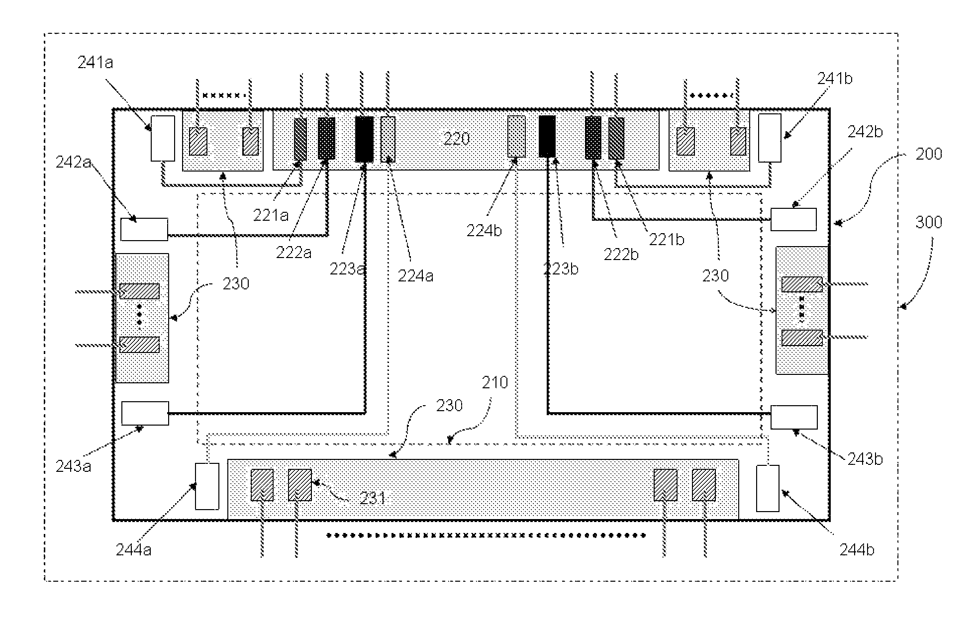
[0019]The main idea of the present invention is to provide a pad layout structure of a driver IC chip, in which dummy power pads and dummy ground pads are disposed on corners of a driver IC chip, and are connected to main power pads and main ground pads, respectively, through metal lines.

[0020]Reference will now be made in greater detail to a preferred embodiment of the invention, an example of which is illustrated in the accompanying drawings. Wherever possible, the same reference numerals will be used throughout the drawings and the description to refer to the same or like parts.

[0021]FIG. 2 is a view illustrating a pad layout structure of a driver IC chip according to an embodiment of the present invention.

[0022]Referring to FIG. 2, a driver IC chip 200 according to an embodiment of the present invention includes an internal circuit 210 disposed at the center of the driver IC chip 200; an input pad part 220 disposed on an outer upper side of the internal circuit 210; and an outpu...


PUM


Abstract

A pad layout structure of a driver IC chip of a liquid crystal display device includes dummy power pads and dummy ground pads, which are disposed in corners of the driver IC chip and are connected to main power pads and main ground pads by metal lines in a chip-on-film (COF) package. Accordingly, it is possible to reduce the resistance of power supply lines and ground lines, to minimize a power dip of a block located far away from the main power pads and main ground pads, and to prevent a failure in power application, which may occur due to a decrease of adhesive strength at a specific position, by dispersing the adhesion positions of the power pads and ground pads.

Description

BACKGROUND OF THE INVENTION[0001]1. Field of the Invention[0002]The present invention relates to a pad layout structure of a driver IC chip of a liquid crystal display device, and more particularly, to a pad layout structure of a driver IC chip in which dummy power pads and dummy ground pads are disposed in corners of a driver IC chip, and are connected to main power pads and main ground pads by metal lines in a chip-on-film (COF) package.[0003]2. Description of the Related Art[0004]A Liquid Crystal Display (LCD) is a device for displaying image data by allowing light to pass through the liquid crystal based on the characteristic of liquid crystal molecules, in which the arrangement thereof changes depending on an applied voltage. Among various LCDs, recently, a Thin Film Transistor (TFT) LCD formed using silicon IC fabrication technology has been the most actively used.[0005]The TFT-LCD includes a liquid crystal panel and a driver IC for driving the liquid crystal panel. The liquid...

Claims


Application Information

Patent Timeline
Patent Type & Authority Patents(United States)
IPC IPC(8): H05K7/10H05K7/12
CPCH01L24/06H01L2224/05599H01L2224/85399H01L2924/01004H01L2924/01014H01L2924/01033H01L2924/14H01L2924/00014H01L2924/01006H01L2224/45099H01L23/50H01L23/48
Inventor CHOI, JOUNG CHEULNA, JOON HOKIM, DAE SEONG
Owner SILICON WORKS CO LTD
Why Eureka
Try Eureka