

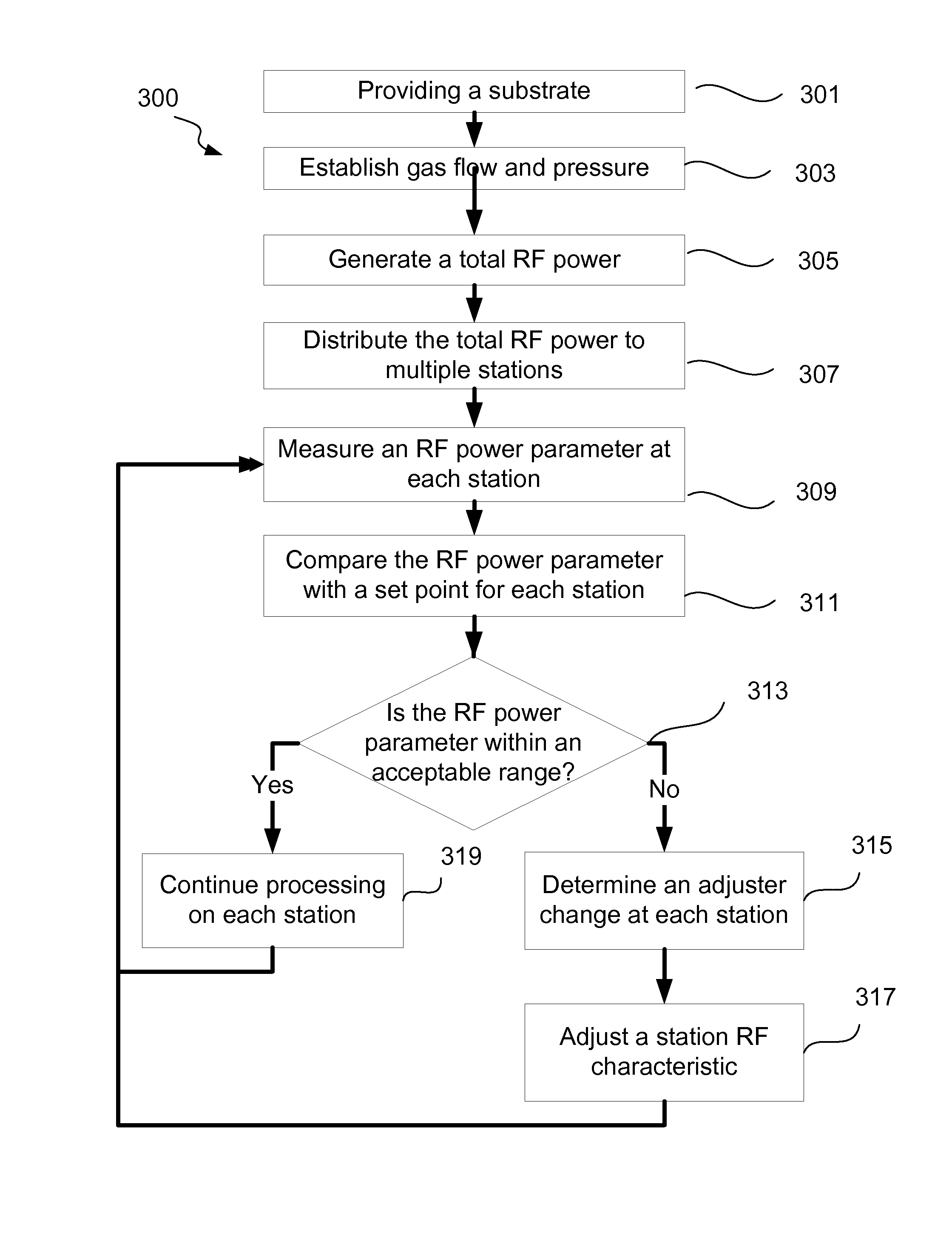
Closed loop control system for RF power balancing of the stations in a multi-station processing tool with shared RF source
a technology of closed loop control system and processing tool, which is applied in the direction of coating, coating, chemical vapor deposition coating, etc., to achieve the effect of reducing process variation in rf-based semiconductor processes, high impedance of delivery circuit, and approximating power balan
- Summary
- Abstract
- Description
- Claims
- Application Information
AI Technical Summary
Benefits of technology
Problems solved by technology
Method used
Image

Examples
example
[0047]Actual station HF RF power data was collected on a Vector Extreme system, available from Novellus Systems of San Jose, Calif. FIGS. 4A and 4B are plots of the station RF power (Watts) measured over time (arbitrary units). FIG. 4A shows measurement for four stations A (401), B (402), C (403), and D (404) without any RF power balancing. As described above, the RF power changed over time. Stations A and C (as shown by lines 401 and 403) have station RF powers that overlap considerably. Stations B and D (as shown by liens 402 and 404) have station RF powers that differ from that of stations A and C and from each other.
[0048]After the station RF power data was collected, capacitors associated with each station were manually tuned to bring all RF powers to the same level. FIG. 4B is a plot of station RF powers collected after the capacitor tuning. For most of the curve, lines 401 to 404, corresponding to stations A to D, are indistinguishable. An initial spike 405 was recorded for s...
PUM
| Property | Measurement | Unit |
|---|---|---|
| Power | aaaaa | aaaaa |
| Electrical inductance | aaaaa | aaaaa |
| Electric potential / voltage | aaaaa | aaaaa |
Abstract
Description
Claims
Application Information