Methods of forming microdevice substrates using double-sided alignment techniques

a technology of alignment technique and micro-device, applied in the direction of photomechanical treatment, instruments, electrical equipment, etc., can solve the problem that the indirect alignment process may not provide sufficient alignment accuracy

Active Publication Date: 2012-10-09
INTEGRATED DEVICE TECH INC
View PDF6 Cites 10 Cited by
  • Summary
  • Abstract
  • Description
  • Claims
  • Application Information

AI Technical Summary

Benefits of technology

[0007]According to still further embodiments of the invention, a method of forming a substrate having microelectromechanical resonators therein may include selectively etching a first surface of the substrate having a plurality of resonator device structures therein to define at least one alignment key therein that extends partially through the substrate. A second surface of the substrate is then recessed to expose the at least one alignment key. At least one photolithographically defined pattern is formed in the second surface by aligning a photolithography mask to the at least one alignment key at the second surface. According to some of these embodiments of the invention, the recessing includes chemically-mechanically polishing the second surface of the substrate to expose the at least one alignment key. Alternatively, the recessing may include thermally oxidizing the second surface of the substrate for a sufficient duration to define an optically transparent oxide layer on the second surface that exposes the at least one alignment key. In additional embodiments of the invention, the step of forming at least one photolithographically defined pattern may include selectively removing portions of the optically transparent oxide layer to expose the second surface. Moreover, in the event one or more non-transparent layers are deposited on the optically transparent oxide layer, which render the alignment keys non-visible to photolithographic imaging equipment, then respective portions of these non-transparent layers can be removed using a relatively low-accuracy photolithographic masking step to thereby expose the alignment keys.

Problems solved by technology

Unfortunately, this indirect alignment process may not provide sufficient alignment accuracy for applications requiring a high degree of alignment between the first and second device structures on opposing sides of a substrate (e.g., semiconductor wafer).

Method used


Image

  • Methods of forming microdevice substrates using double-sided alignment techniques
  • Methods of forming microdevice substrates using double-sided alignment techniques
  • Methods of forming microdevice substrates using double-sided alignment techniques

Examples


Embodiment Construction

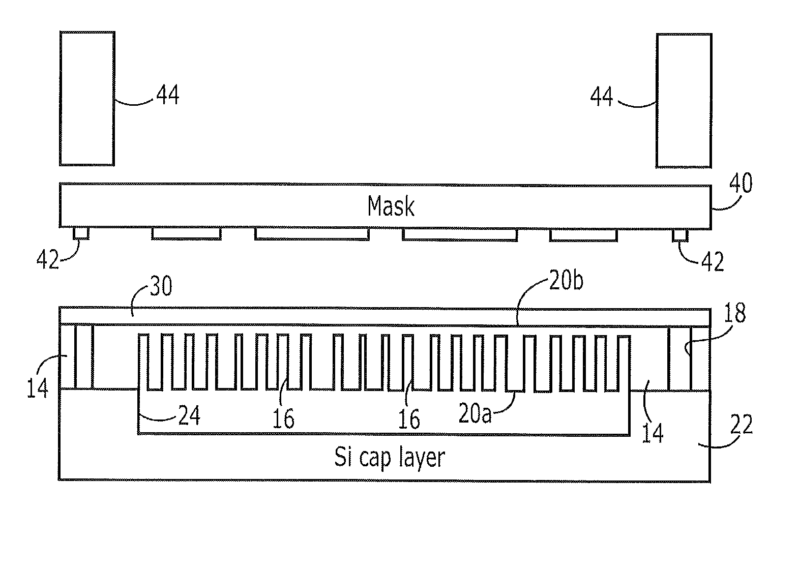
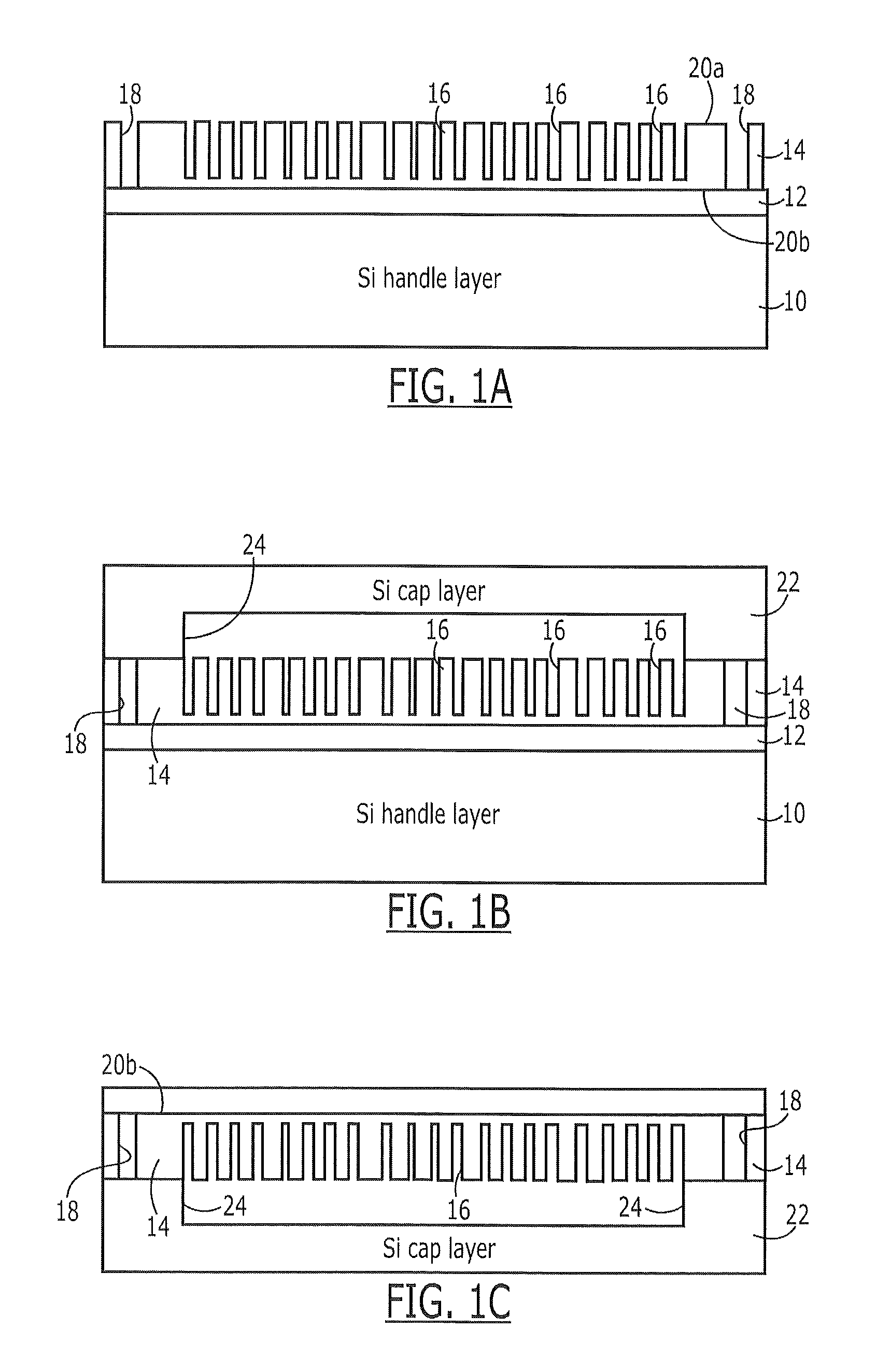
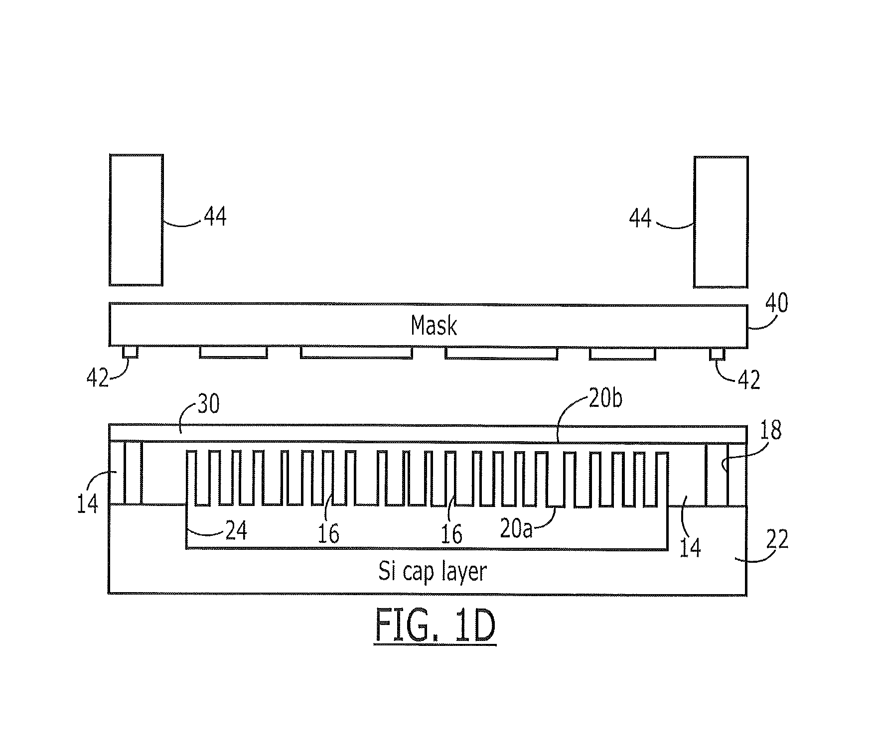
[0010]The present invention now will be described more fully with reference to the accompanying drawings, in which preferred embodiments of the invention are shown. This invention may, however, be embodied in many different forms and should not be construed as being limited to the embodiments set forth herein; rather, these embodiments are provided so that this disclosure will be thorough and complete, and will fully convey the scope of the invention to those skilled in the art. Like reference numerals refer to like elements throughout.

[0011]It will be understood that when an element or layer is referred to as being “on,”“connected to” or “coupled to” another element or layer (and variants thereof), it can be directly on, connected or coupled to the other element or layer or intervening elements or layers may be present. In contrast, when an element is referred to as being “directly on,”“directly connected to” or “directly coupled to” another element or layer (and variants thereof),...


PUM


Abstract

Methods of forming substrates having two-sided microstructures therein include selectively etching a first surface of the substrate to define a plurality of alignment keys therein that extend through the substrate to a second surface thereof. A direct photolithographic alignment step is then performed on a second surface of the substrate by aligning a photolithography mask to the plurality of alignment keys at the second surface. This direct alignment step is performed during steps to photolithographically define patterns in the second surface.

Description

FIELD OF THE INVENTION[0001]The present invention relates to microdevice fabrication techniques and, more particularly, to microdevice fabrication techniques that use double-sided alignment processes to define structures on opposing surfaces of a substrate.BACKGROUND OF THE INVENTION[0002]Many microfabrication processes require the formation of device structures on opposing sides of a substrate, such as a semiconductor wafer or layer. In one conventional microfabrication process, an image of alignment marks on a first mask is captured during the formation of first device structures in a first surface of the substrate using the first mask and photolithographic processing techniques. Then, during the formation of second device structures in a second surface of the substrate, an alignment step is performed indirectly based on the captured image rather than directly from a mask. During this alignment step, the captured image is aligned to alignment marks on the second surface. Unfortuna...

Claims


Application Information

Patent Timeline
Patent Type & Authority Patents(United States)
IPC IPC(8): H01L21/302H01L21/461
CPCB81C1/00603
Inventor PAN, WANLINGBHUGRA, HARMEET
Owner INTEGRATED DEVICE TECH INC
Why Eureka
Try Eureka