Solid state Klystron

a solid-state klystron and vacuum tube technology, applied in the field of solid-state klystron structures, can solve the problems of bulky vacuum tube devices that cannot be easily integrated with solid-state devices, and achieve the effect of reducing the size of the vacuum tube devi

Inactive Publication Date: 2012-10-09
GLOBALFOUNDRIES INC
View PDF1 Cites 10 Cited by
  • Summary
  • Abstract
  • Description
  • Claims
  • Application Information

AI Technical Summary

Problems solved by technology

Obviously, vacuum tube Klystrons are bulky vacuum tube devices that cannot be easily integrated with solid state devices in a circuit despite their excellent ultra-high frequency amplification characteristics.

Method used


Image

  • Solid state Klystron
  • Solid state Klystron
  • Solid state Klystron

Examples


Embodiment Construction

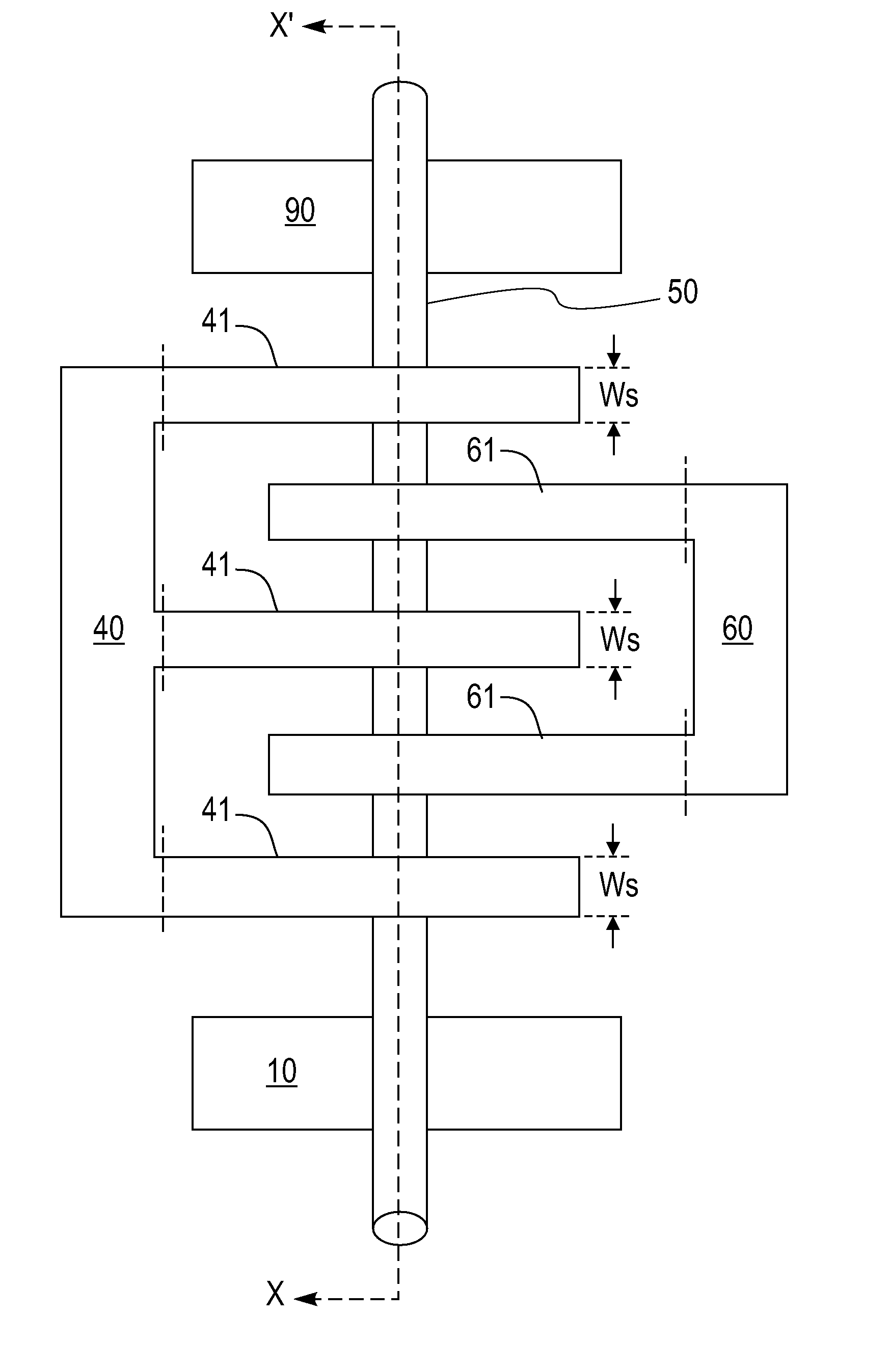
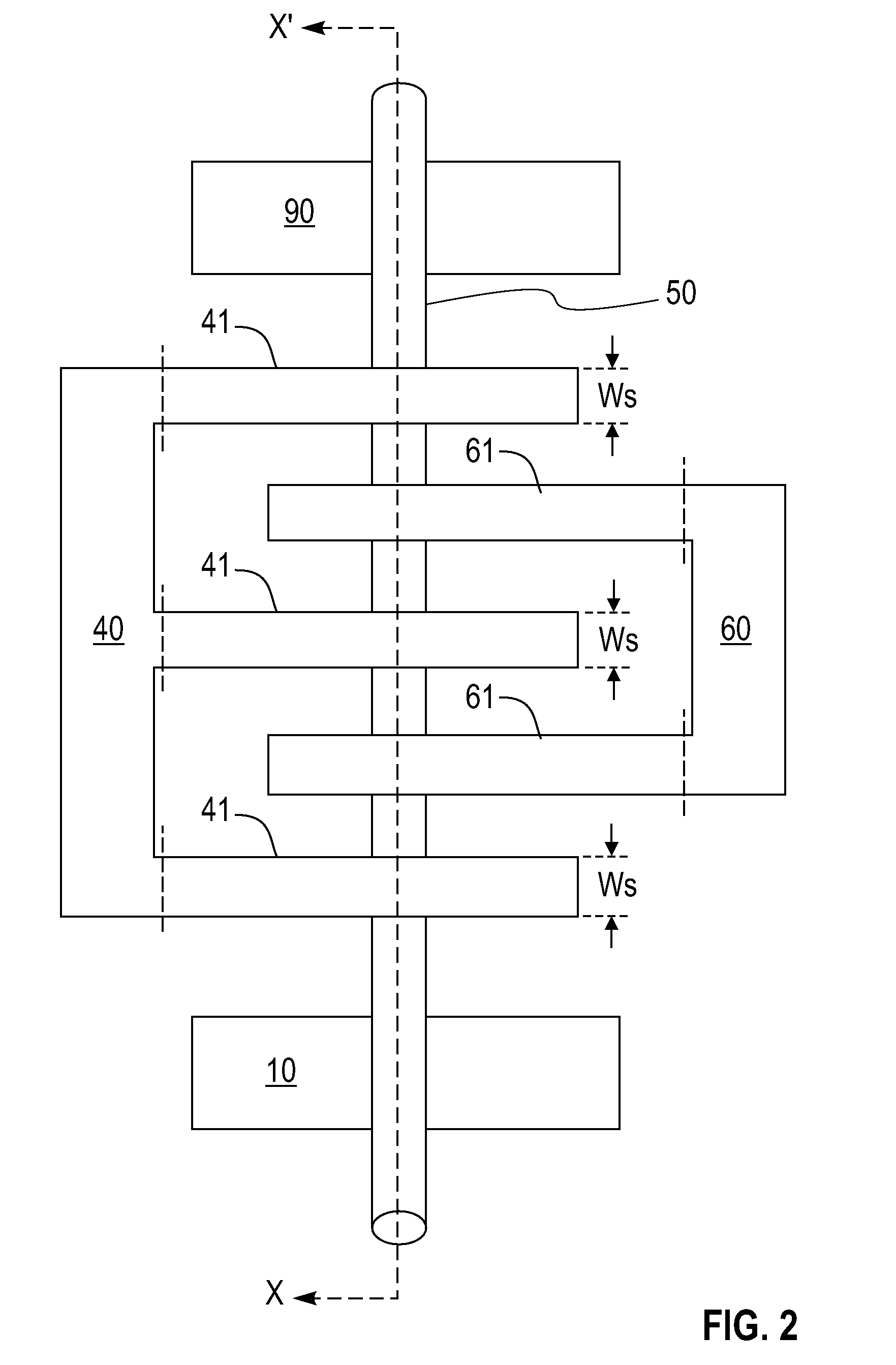
[0060]As stated above, the present invention relates to solid state Klystron structures and methods of manufacturing and operating the same, which is now described in detail with accompanying figures.

[0061]Referring to FIG. 2, a top-down view of an exemplary solid state Klystron comprising a conducting wire 50, source contact 10, a drain contact 90, a bias gate 60 having two bias fingers 61, and a signal gate 40 having three signal fingers 41 is shown. The carriers, e.g., electrons or holes, flow from the source contact 10, through the conducting wire 50, to the drain contact 90 in a ballistic transport by an applied suitable first DC voltage bias between the drain contact 90 and the source contact 10. To facilitate the ballistic transport of the carriers, the material for the conducting wire 50 is chosen such that ballistic mean free paths within the conducting wire 50 are long, that is, comparable to the dimension of the length of the conducting wire 50. The carriers are provided ...


PUM


Abstract

A solid state Klystron structure is fabricated by forming a source contact and a drain contact to both ends of a conducting wire and by forming a bias gate and a signal gate on the conducting wire. The conducting wire may be at least one carbon nanotube or at least one semiconductor wire with long ballistic mean free paths. By applying a signal at a frequency that corresponds to an integer multiple of the transit time of the ballistic carriers between adjacent fingers of the signal gate, the carriers are bunched within the conducting wire, thus amplifying the current through the solid state Klystron at a frequency of the signal to the signal gate, thus achieving a power gain.

Description

FIELD OF THE INVENTION[0001]The present invention relates to semiconductor structures and method of manufacturing and operating the same, and particularly to solid state Klystron structures and methods of manufacturing and operating the same.BACKGROUND OF THE INVENTION[0002]With the realization that end of scaling for conventional complementary metal-oxide-semiconductor (CMOS) integrated circuits is fast approaching in the semiconductor industry, alternative nanostructures and materials have been investigated. Of such nanostructures and materials, carbon nanotubes (CNTs) offer excellent intrinsic properties that are suitable for high performance nanoscale devices.[0003]A key advantage of CNTs over conventional CMOS devices is that scaling limitations of metal-oxide-semiconductor field effect transistors (MOSFETs) due to boundary scattering of electrons from imperfect interfaces are solved naturally in CNTs which have a smooth, well coordinated graphene structure with no bonds to the...

Claims


Application Information

Patent Timeline
Patent Type & Authority Patents(United States)
IPC IPC(8): H01L27/148
CPCH01J25/10B82Y10/00
Inventor SOLOMON, PAUL M.
Owner GLOBALFOUNDRIES INC
Why Eureka
Try Eureka