Semiconductor device, method of manufacturing the same and adsorption site blocking atomic layer deposition method

a technology of atomic layer deposition and semiconductors, applied in the direction of capacitors, electrical appliances, basic electric elements, etc., can solve the problems of increasing leakage current, inability to obtain sufficient thermal stability, and not revealing the control of molar fractions within the specific range, so as to suppress the influence of size effects and good crystallinity

Inactive Publication Date: 2012-10-16
ELPIDA MEMORY INC +1
View PDF5 Cites 8 Cited by
  • Summary
  • Abstract
  • Description
  • Claims
  • Application Information

AI Technical Summary

Benefits of technology

[0042]An important technical object is to provide a semiconductor device and a method of manufacturing the same capable of forming a film on a lower electrode of a capacitor having a steric structure and an aspect ratio of 20 or more with good coverage under process conditions of a high temperature (240° C. to 300° C.) to increase a permittivity, and preventing ZrO2 crystals from being separated by an Al-doped layer by precisely adding an appropriate amount of Al.
[0044](1) An Al-doped dielectric film (including metal atoms M except for Al) is formed by an ALD method at a relatively high temperature (240° C. to 300° C.), and a concentration of Al added to improve thermal stability (Al / (Al+M)) is set to be 0.2 to 2 atom %.
[0061]According to the present invention, it is possible to a dielectric film having good crystallinity, suppress an influence of the size effects, and have an area density at an Al-doped layer at which the dielectric film is not divided.
[0062]Further, according to a manufacturing method of the present invention, it is possible to achieve the area density.

Problems solved by technology

In this case, it is impossible to obtain sufficient thermal stability by using a monolithic dielectric film of a zirconium oxide film and there is a problem of increasing leakage current after heat treatment.
Further, it does not disclose how to control molar fractions within the specific range.
However, in a capacitor for DRAM since F value of 40 nm, it is considered that an aspect ratio of 35 is a limitation achievable by one dry etching in the current processing technology.
However, the Zr source disclosed in the above-mentioned prior art documents is self-decomposed by heat in the film formation at a high temperature at which a tetragonal structure is obtained, and coverage is deteriorated.
Consequently, since it is impossible to reduce the EOT, the permittivity is hardly to be compatible with the coverage.
This is because if the amount of Al is excessively large, it is hardly to obtain a film having high permittivity, and if the amount of Al is excessively small, it is hardly to obtain sufficient thermal stability.
However, in the film formation at a high temperature, the coverage is deteriorated as described in 1) above.
As a result, even though a total film thickness is 6 nm or more, the permittivity of each of the ZrO2 films divided by the Al2O3 layer is reduced by the size effects, and it is difficult to make the EOT of the total dielectric film small.
Further, although Al doping was performed by selecting one ALD cycle of a ZrxAlyOz film disclosed in JP 2007-150242A and using the Zr source disclosed in the conventional technology, it was impossible to suppress the division of the ZrO2 film.
As described above, it is difficult to avoid the division of the ZrO2 film in the ZAZ structure by a conventional combination of the Zr source and the Al source and a conventional sequence.

Method used


Image

  • Semiconductor device, method of manufacturing the same and adsorption site blocking atomic layer deposition method
  • Semiconductor device, method of manufacturing the same and adsorption site blocking atomic layer deposition method
  • Semiconductor device, method of manufacturing the same and adsorption site blocking atomic layer deposition method

Examples


Embodiment Construction

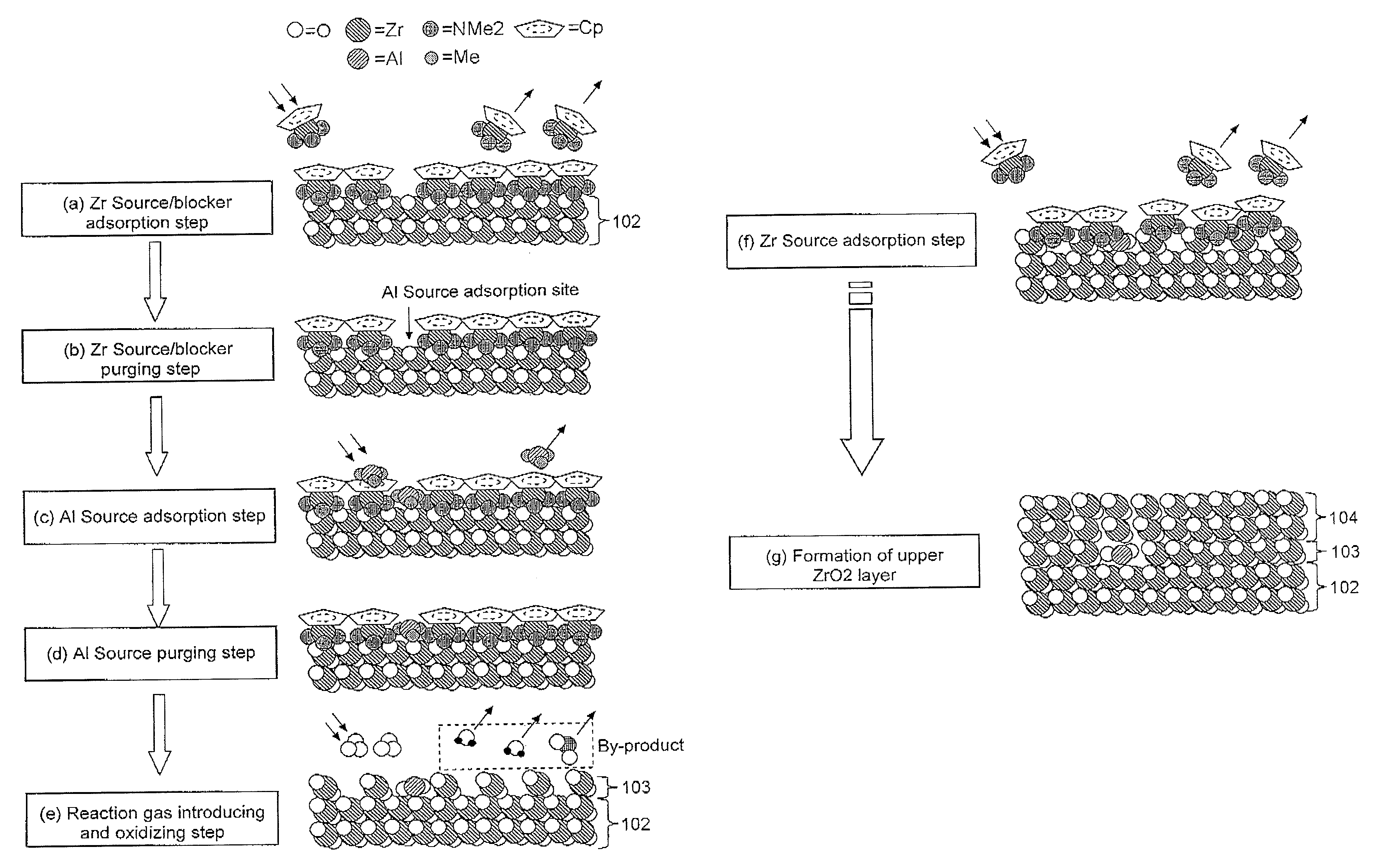
[0083]The invention will be now described herein with reference to illustrative embodiments. Those skilled in the art will recognize that many alternative embodiments can be accomplished using the teachings of the present invention and that the invention is not limited to the embodiments illustrated for explanatory purpose.

[0084]Hereinafter, embodiments of the present invention will be described in comparison with conventional techniques.

[0085]First, two conventional techniques of “Al doping method B” and “Al doping method C” will be described for comparison.

[0086]

[0087]First, one of conventional techniques based on a method disclosed in JP 2006-135339A or JP 2007-73926A will be described. Hereinafter, this is referred to as “Al doping method B” for convenience.

[0088]The Al doping method B is close to a stacking structure of a ZrO2 film and Al2O3 film rather than doping. That is, the ZrO2 film is obtained by repeating, as many times as desired, the steps of (1) introducing a Zr sour...


PUM

PropertyMeasurementUnit
temperatureaaaaaaaaaa
feature sizeaaaaaaaaaa
relative permittivityaaaaaaaaaa

Abstract

To provide a dielectric film having good crystallinity while suppressing an influence of the size effects and preventing the dielectric film from being divided by an Al-doped layer although there is provided the Al-doped layer for improving the leakage characteristics in the dielectric film of a capacitor, the dielectric film has at least one Al-doped layer, and an area density of Al atoms in one layer of the Al-doped layer is smaller than 1.4E+14 atoms / cm2. Further, to achieve the area density, there is employed a combination of formation of a dielectric film using a general ALD method and Al doping using an adsorption site blocking ALD method including adsorbing a blocker molecule restricting an adsorption site of an Al source, adsorbing the Al source, and introducing a reaction gas for reaction.

Description

BACKGROUND OF THE INVENTION[0001]1. Field of Invention[0002]The present invention relates to a semiconductor device and a method of manufacturing the same, and specifically, to a semiconductor device having a capacitor, particularly, a dielectric film used for the capacitor and a method of manufacturing the same. Further, the present invention relates to a novel atomic layer deposition (ALD) method appropriate for introducing impurities in low concentration.[0003]2. Description of Related Arts[0004]As one of dielectric materials of a capacitor for a dynamic random access memory (DRAM), there is zirconium oxide (ZrO2).[0005]The DRAM requires heat treatment at a temperature of about 450° C. to 500° C. as an inevitable process after formation of a capacitor. In this case, it is impossible to obtain sufficient thermal stability by using a monolithic dielectric film of a zirconium oxide film and there is a problem of increasing leakage current after heat treatment.[0006]Accordingly, vari...

Claims


Application Information

Patent Timeline
Patent Type & Authority Patents(United States)
IPC IPC(8): H01L21/02
CPCH01L21/02178H01L21/02186H01L28/40H01L21/022H01L21/0228H01L21/02189H01L21/205H10B99/00H10B12/00
Inventor HIROTA, TOSHIYUKIKIYOMURA, TAKAKAZUMOROZUMI, YUICHIROHISHIYA, SHINGO
Owner ELPIDA MEMORY INC
Why Eureka
Try Eureka