Liquid crystal display apparatus, drive method thereof, and liquid crystal projection apparatus

a technology of liquid crystal display and drive method, which is applied in the direction of non-linear optics, static indicating devices, instruments, etc., can solve the problems of two-connected pixel defects and markable image quality deterioration, and achieve the effect of suppressing image quality deterioration and reducing image quality deterioration

Inactive Publication Date: 2012-10-16
CANON KK
View PDF11 Cites 0 Cited by
  • Summary
  • Abstract
  • Description
  • Claims
  • Application Information

AI Technical Summary

Benefits of technology

[0011]The present invention is directed to suppress the deteriorations of an image quality owing to parasitic capacitance coupling between pixel electrodes and a feedthrough between pixels, and to suppress the deterioration of the image quality owing to the occurrence of a pixel defect over a plurality of rows.
[0014]The present invention can suppress the deteriorations of image quality owing to the parasitic capacitance coupling between pixel electrodes and a feedthrough between pixels, and can suppress the deterioration of the image quality owing to the occurrence of a pixel defect over a plurality of rows.

Problems solved by technology

However, the related art described above has the following problem.
As a result, a remarkable image quality deterioration is caused.
Consequently, a two-connected pixel defect is caused in the vertical scan drive, which turns on two rows simultaneously.

Method used


Image

  • Liquid crystal display apparatus, drive method thereof, and liquid crystal projection apparatus
  • Liquid crystal display apparatus, drive method thereof, and liquid crystal projection apparatus
  • Liquid crystal display apparatus, drive method thereof, and liquid crystal projection apparatus

Examples


first embodiment

(First Embodiment)

[0026]FIG. 3 is a diagram illustrating a circuit example of a liquid crystal display apparatus by a first embodiment of the present invention. In the following, the liquid crystal display apparatus and a drive method thereof will be described. The liquid crystal display apparatus includes a plurality of unit pixels 100 constituting the display area of the liquid crystal display apparatus. The unit pixels 100 are arranged in a matrix, each including a switch element 101, a pixel holding capacitor 102, and a liquid crystal 104. A MOS transistor is used as the switch element 101 in the present embodiment here. The counter electrode of the pixel holding capacitor 102 is at a first reference voltage 103, which is commonly used for all of the pixels. Although not illustrated, an electrode is arranged at a connection end of the switch element 101 and the pixel holding capacitor 102, and the liquid crystal 104 is arranged to be put between the electrode and a transparent e...

second embodiment

(Second Embodiment)

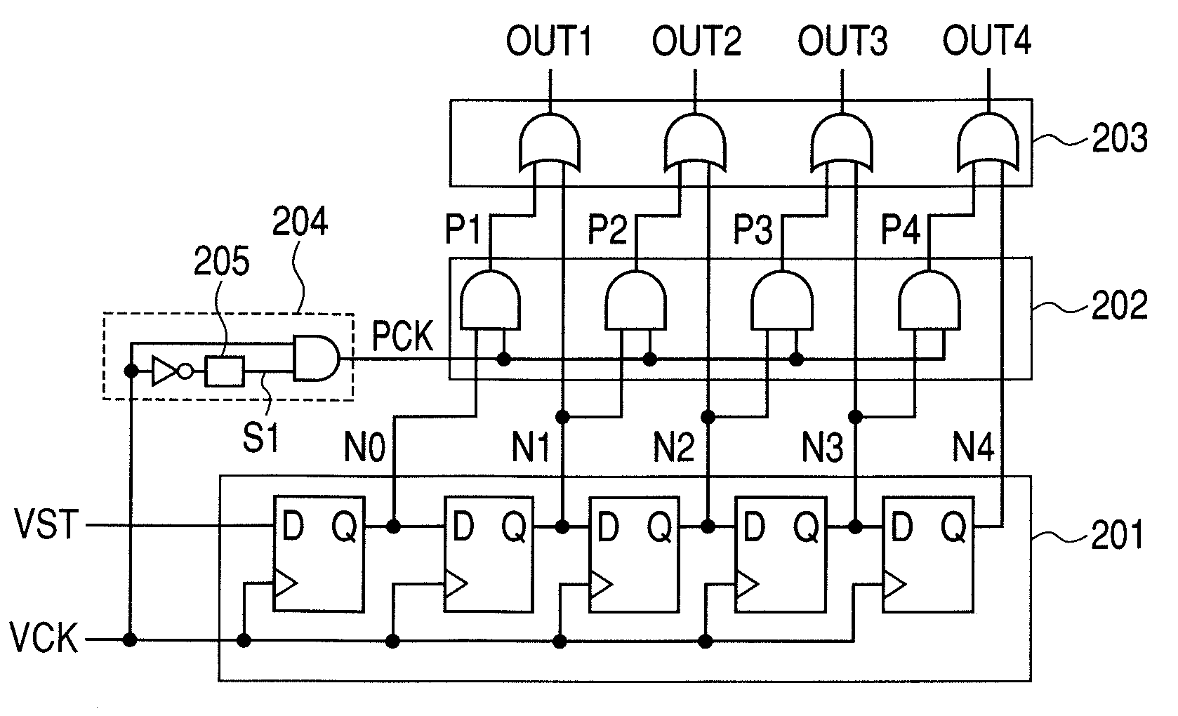
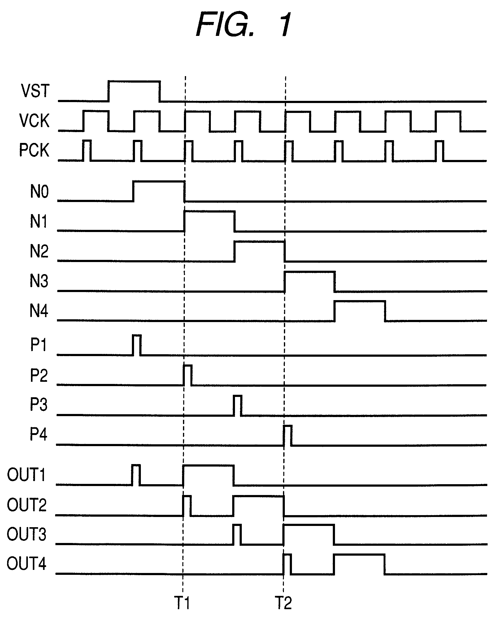
[0049]FIG. 5 is a diagram illustrating a second embodiment of the vertical scan circuit 110 illustrated in FIG. 3. The feature of the present embodiment is that the control clock signal PCK is generated by a third signal generating circuit 204 in the substrate on the basis of the vertical scan clock signal VCK. Because the other parts of the present embodiment are the same as those of the first embodiment except the addition of the third signal generating circuit 204, the descriptions of the other parts are omitted.

[0050]Next, the configuration of the third signal generating circuit 204 will be described. The vertical scan clock signal VCK is input into an input terminal of an inverter circuit (hereinafter referred to as INV circuit) and one input terminal of an AND circuit, and an output of the INV circuit is input into the other input terminal of the AND circuit through a delay circuit 205. The delay circuit 205 may be either of (a) an analog delay circuit using...

third embodiment

(Third Embodiment)

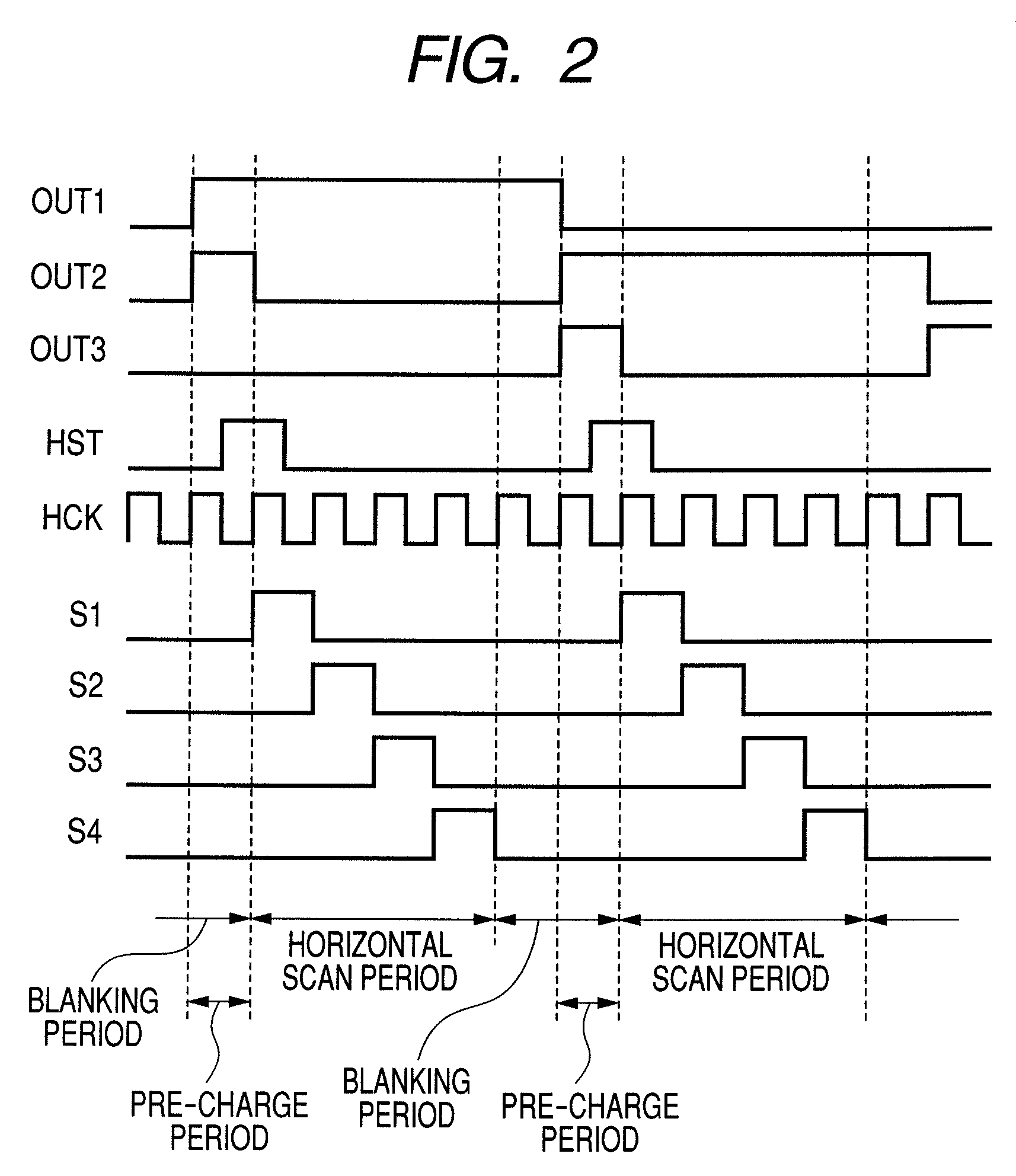
[0053]FIG. 7 is a third embodiment of the vertical scan circuit 110 illustrated in FIG. 3. The vertical scan circuit 110 illustrated in the present embodiment differs from that illustrated in the first embodiment in the following three points: a fourth signal generating circuit 206 is provided between the shift register circuit 201 and the second signal generating circuit 203; the output signals S1-S4 of the fourth signal generating circuit 206 are input into the other input terminals of the AND circuits in the second signal generating circuit 203; and the shift register circuit 201 is made up of latch circuits, each composed of two tri-state inverters and one inverter.

[0054]FIG. 8 illustrates the circuit for one bit of the shift register circuit 201 used in the present embodiment. The circuit enclosed by a dotted line is the so-called tri-state inverter, the output of which is controlled to be high impedance by a control signal CK1, and two tri-state inverters and...


PUM


Abstract

A liquid crystal display apparatus includes: a plurality of pixels arranged in a matrix, each including a switching element connected to a pixel electrode for applying a voltage to a liquid crystal placed between the pixel electrode and a counter electrode; and a vertical scan circuit for supplying a scan signal for controlling the switch element between conducting and non-conducting states, and for scanning the pixels scan line by scan line sequentially, wherein the scan signal includes a first conducting signal setting the switch element at the conducting state, a second conducting signal setting the switch element at the conducting state following to the first conducting signal, and a non-conducting signal setting the switch element at the non-conducting state between the first and second conducting signals to suppress deterioration of the image quality owing to the parasitic capacitance coupling between pixel electrodes and a feedthrough between pixels.

Description

BACKGROUND OF THE INVENTION[0001]1. Field of the Invention[0002]The present invention relates to a liquid crystal display apparatus, a drive method thereof, and a liquid crystal projection apparatus.[0003]2. Description of the Related Art[0004]As an image display apparatus using an active matrix substrate, a liquid crystal display apparatus is known, and the liquid crystal display apparatus is widely adopted to a liquid crystal projector, a liquid crystal display, and the like. As is well known, such a liquid crystal display apparatus using an active matrix substrate includes pixel cells arranged in a matrix on, for example, a semiconductor substrate, and each of the pixel cells includes a pixel switch made of a metal oxide semiconductor (MOS) transistor and a pixel capacitor connected to the pixel switch. That is, a plurality of scan lines is arranged along horizontal directions, and a plurality of signal lines is arranged along vertical directions. Then, a pixel cell is connected ...

Claims


Application Information

Patent Timeline
Patent Type & Authority Patents(United States)
IPC IPC(8): G09G3/36
CPCG09G3/3677G09G2320/0219
Inventor OOMURA, MASANOBU
Owner CANON KK
Why Eureka
Try Eureka