
Trigger circuits and event counters for an IC

a trigger circuit and event counter technology, applied in the direction of instruments, generating/distributing signals, pulse techniques, etc., can solve the problems of less resources for implementing user designs, less sophisticated user designs, and more complicated debug network resources,

Active Publication Date: 2012-10-23
TAHOE RES LTD
View PDF143 Cites 26 Cited by
  • Summary
  • Abstract
  • Description
  • Claims
  • Application Information

AI Technical Summary

Benefits of technology

This approach allows for tailored debugging functionality that reduces resource consumption, provides relevant data to users, and enhances debugging efficiency by filtering out irrelevant data and automating data capture.

Problems solved by technology

However, many such user designs include various design bugs, design defects, or unexpected runtime behavior that pass unseen through design and testing.
In such cases, a more complicated debug network consumes greater resources of the IC, leaving fewer resources for implementing the user design.
As a result, user designs become less sophisticated.
Additionally, a change to either the core logic functionality of the primary circuit structure or the functionality of the debug network could cause the entire IC design to have to be recompiled, downloaded, and loaded onto the IC.
This is due to the fact that changes to a design, even when made on a small scale to localized circuits, could have a design-wide impact affecting the overall circuit routing or timing of the design.
These changes also create the risk that the circuit logic, including seemingly unrelated logic, may be “broken” due to errors in implementing the new functional change.
Because of this risk, extensive regression testing and verification of the logic of the primary circuit structure and debug network is required.
However, implementing the debugging circuitry as fixed-function circuitry also has several drawbacks.
Therefore, the dedicated resources of the debug network go unused and are effectively wasted as these resources cannot be modified to complement the functionality of the primary circuit structure that implements the user design.
Unanticipated usage, behavior, or operating conditions in the field could pose issues beyond the debugging scope of the programmed debug network, forcing users to have to employ third party tools or other means to perform the additional debug functionality needed to handle the unanticipated usage, behavior, or operating conditions.
A further issue prevalent in traditional debug networks is the inability of the networks to provide meaningful debug data to the users.
Debug networks often blindly report data at a debug point within the user design.
As a result, users waste time in deciphering the debug data.

Method used


Image

  • Trigger circuits and event counters for an IC
  • Trigger circuits and event counters for an IC
  • Trigger circuits and event counters for an IC

Examples


Embodiment Construction

[0063]In the following detailed description of the invention, numerous details, examples, and embodiments of the invention are set forth and described. However, it will be clear and apparent to one skilled in the art that the invention is not limited to the embodiments set forth and that the invention may be practiced without some of the specific details and examples discussed.

[0064]I. Overview

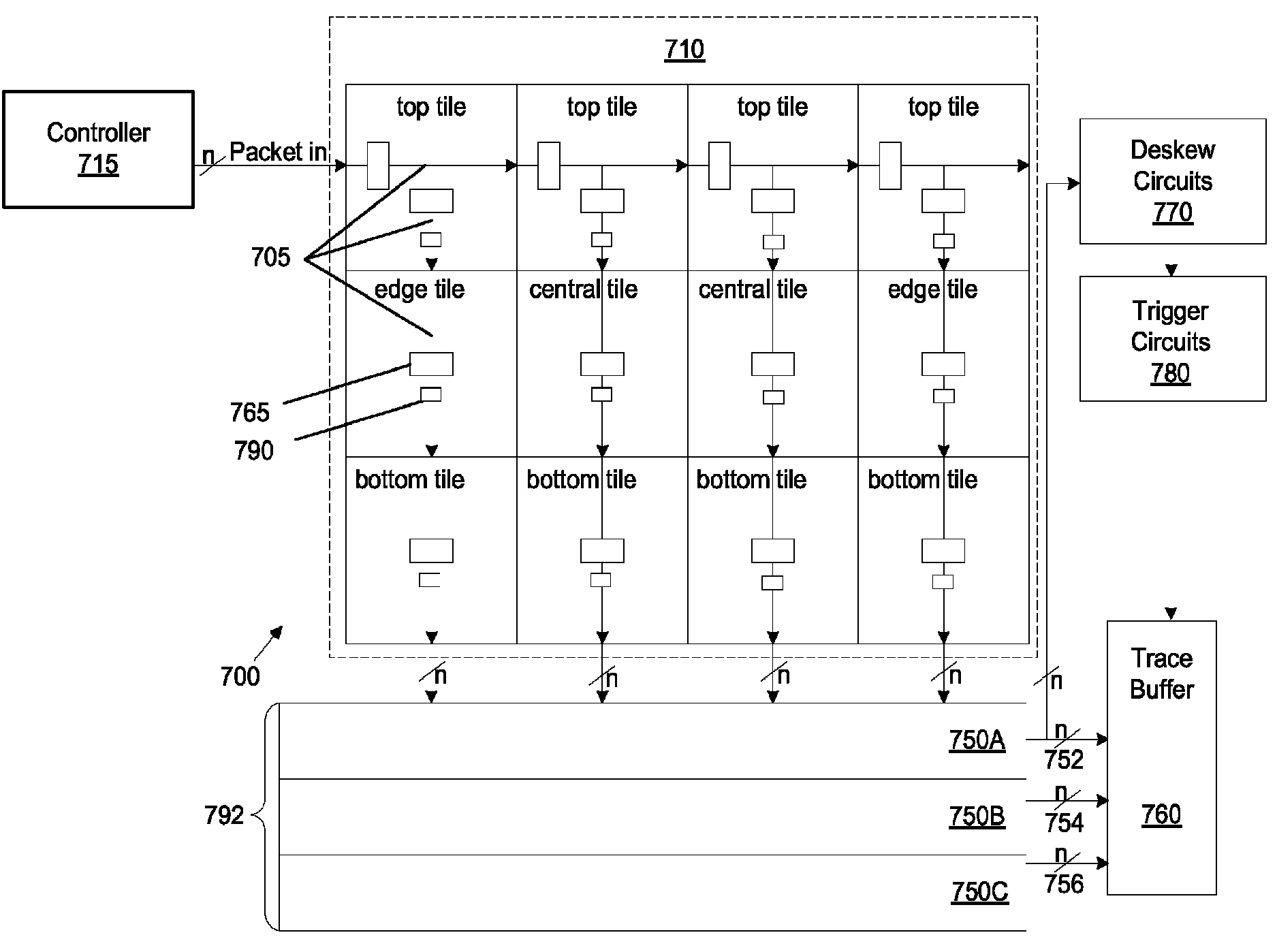
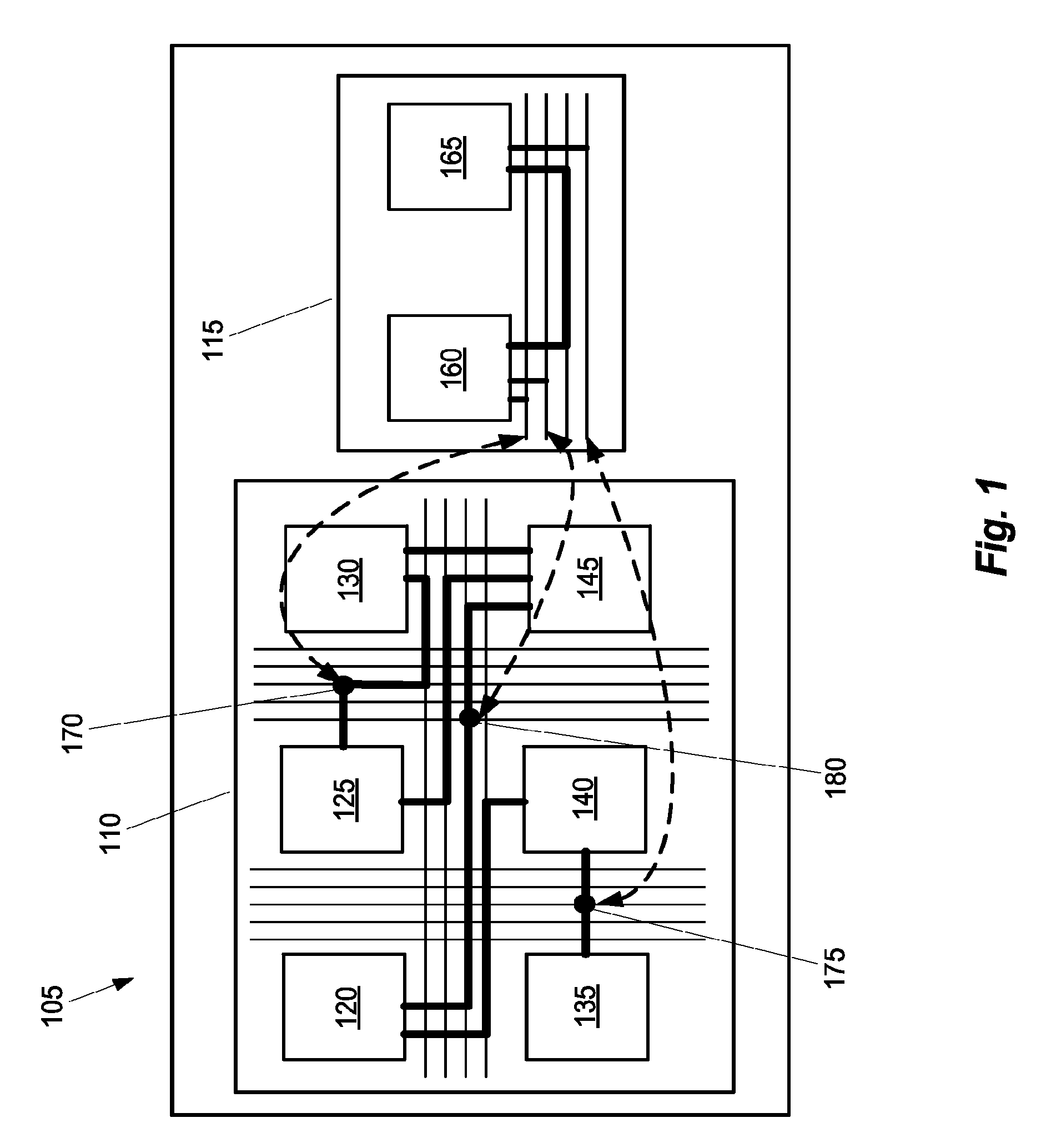
[0065]Some embodiments provide different methods of tracking data values in an integrated circuit (“IC”) by using a secondary circuit structure that is separate from a data routing fabric used to implement a user design. A method of some such embodiments allows a user to select a set of resources to monitor. In some embodiments, signals corresponding to these selected resources are continuously read onto the secondary circuit structure. The method of some embodiments then allows the user to define a trigger event that defines which of these signals will be captured for viewing by the user. The...


PUM


Abstract

Some embodiments provide an integrated circuit (“IC”). The IC includes multiple configurable circuits that configurably perform operations of a user design based on configuration data. The IC also includes a configurable trigger circuit that receives a set of configuration data that specifies an operational event. The configurable trigger circuit also determines whether the operational event has occurred during implementation of the user design of the IC. Additionally, the operational trigger event outputs a trigger signal upon determining that the operational trigger event has occurred.

Description

CLAIM OF BENEFIT TO PRIOR APPLICATIONS[0001]This application is a continuation application of PCT Application PCT / US2008 / 088492, entitled “Trigger Circuits and Event Counters for an IC,” filed on Dec. 29, 2008, now published as WO 2010 / 016857. PCT Application PCT / US2008 / 088492 claims the benefit of U.S. Provisional Patent Application 61 / 086,145, entitled “GUI for Tracking Data Values in an IC,” filed Aug. 4, 2008 and U.S. Provisional Patent Application 61 / 098,732, entitled “Trigger Circuits and Event Counters for a Monitoring Network of a Configurable IC,” filed Sep. 19, 2008. U.S. Provisional Patent Applications 61 / 086,145 and 61 / 098,732 and PCT Application PCT / US2008 / 088492, published as WO 2010 / 016857, are incorporated herein by reference.FIELD OF THE INVENTION[0002]The present invention is directed towards efficiently debugging an IC using a secondary network of the IC.BACKGROUND OF THE INVENTION[0003]Configurable integrated circuits (“ICs”) arc programmable and can be used to i...

Claims


Application Information

Patent Timeline
Patent Type & Authority Patents(United States)
IPC IPC(8): G06M3/00
CPCG06M3/00G06F1/04H03K19/17736H03K19/17728H03K19/1776H03K19/017581H03K19/17764H03K19/17748
Inventor HUTCHINGS, BRADREDGRAVE, JASONHUANG, DAITEIG, STEVEN
Owner TAHOE RES LTD
Learn More