Illuminating means

a technology of illumination means and light sources, applied in the direction of basic electric elements, electrical apparatus, semiconductor devices, etc., can solve the problems of increasing the cost of illumination means on the one hand, limiting function, and not being able to replace in the event of damag

Inactive Publication Date: 2012-11-06
VICTORINOX
View PDF19 Cites 0 Cited by
  • Summary
  • Abstract
  • Description
  • Claims
  • Application Information

AI Technical Summary

Benefits of technology

[0010]In the case of known illuminating means, semiconductor components are usually disposed on the support base in a manner which makes the production process simple and practicable and they are disposed in the optical center, and the optical center usually coincides with the center point or line of symmetry. In particular, however, the contact points are usually disposed at an identical distance from a line of symmetry or from the center point. As a result of this arrangement, however, a shadow is created in the region of the portion of the semiconductor components emitting the light, which leads to a portion with a significantly reduced radiation intensity in the emitted light beam.
[0023]One advantageous embodiment can be obtained in which the support base and the electrode arrangement are disposed in a housing and the housing is made from a light-guiding material. The advantage of providing a housing is that the semiconductor components are provided with sufficient mechanical protection and the process of assembling or fitting the illuminating means in another module is made much easier. If the housing is made from a light-guiding material, a particular advantage is obtained because light can already be deflected or light collected by this material, which again enables the optical efficiency of the illuminating means proposed by the invention to be improved. The light-guiding material may also be designed to produce specific spectral filtering for example, in which case undesired spectral components can be filtered out and as narrow a spectral range as possible can be emitted. However, the light-guiding material may also be of the type designed to produce diffuse scattering so that an illuminating effect can be achieved in as wide as possible a spatial range by reference to an optical axis of the illuminating means.

Problems solved by technology

Due to the high degree of integration, however, replacement in the event of damage is usually not possible or is so to a very limited degree only.
If an illuminating means fails, this can therefore lead to a restriction in function, as a result of which additional illuminating means not intended for the specific function are provided as a replacement in a known manner.
During operation for the intended function, these illuminating means are not active and are not switched on unless an illuminating means is damaged, thereby increasing the cost of the illuminating means on the one hand and also requiring additional space in order to accommodate it.
Known illuminating means based on semiconductor modules have a particular disadvantage in that, because of the electrical contact needed, a part-portion of the light-emitting surface is placed in shadow by the contact point.
As a result, the image irradiated by such illuminating means has a region with significantly reduced radiation intensity, which is a disadvantage in terms of generating illumination that is as uniform as possible.

Method used


Image

  • Illuminating means
  • Illuminating means
  • Illuminating means

Examples


Embodiment Construction

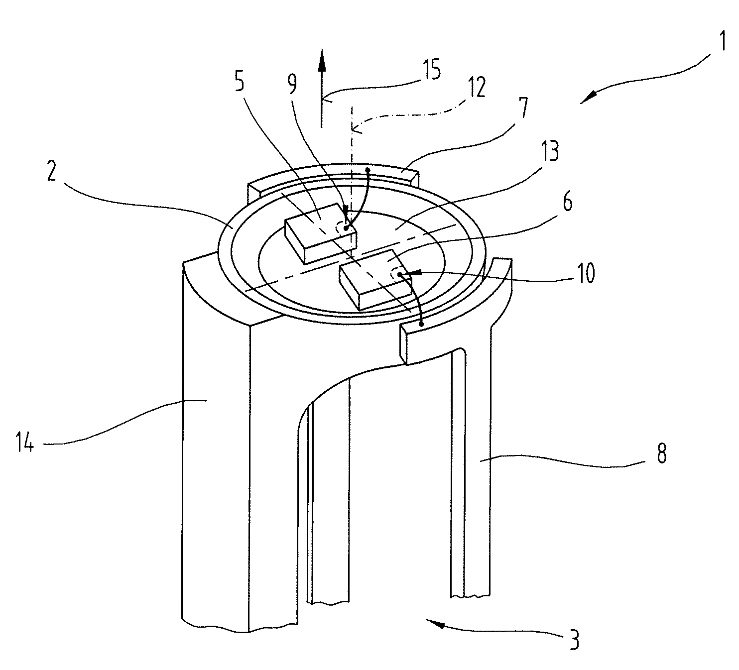
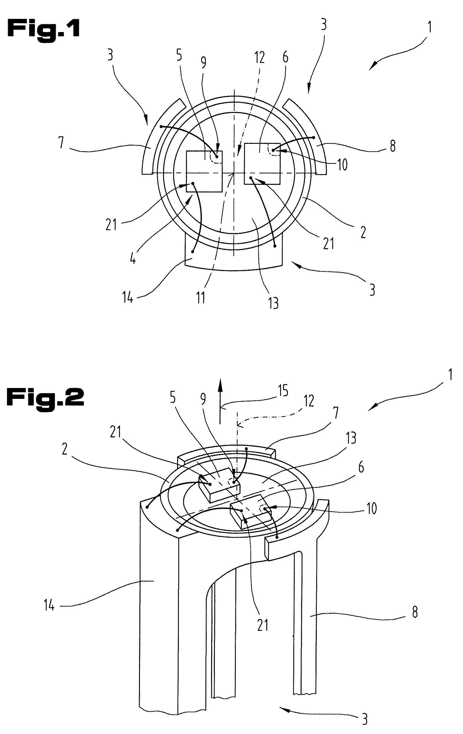
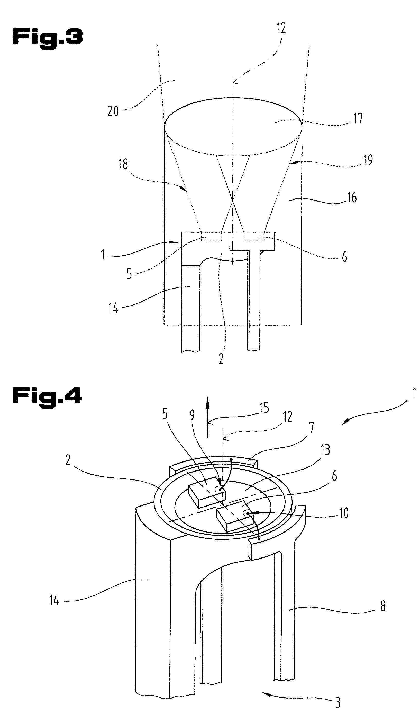
[0033]Firstly, it should be pointed out that the same parts described in the different embodiments are denoted by the same reference numbers and the same component names and the disclosures made throughout the description can be transposed in terms of meaning to same parts bearing the same reference numbers or same component names. Furthermore, the positions chosen for the purposes of the description, such as top, bottom, side, etc., relate to the drawing specifically being described and can be transposed in terms of meaning to a new position when another position is being described. Individual features or combinations of features from the different embodiments illustrated and described may be construed as independent inventive solutions or solutions proposed by the invention in their own right.

[0034]All the figures relating to ranges of values in the description should be construed as meaning that they include any and all part-ranges, in which case, for example, the range of 1 to 1...


PUM


Abstract

An illuminating means, including a radiation source for emitting electromagnetic radiation in the optical range, a support base, and an electrode arrangement with a first and at least a second electrode. The radiation source is disposed on the support base and connected by connecting wires to the electrode arrangement so as to be electrically conductive, and the radiation source is provided in the form of a first and at least a second semiconductor component. The first electrode is connected to the first semiconductor component via a first contact point, and the second electrode is connected to the second semiconductor component via a second contact point, so as to be electrically conductive. The distance of the first contact point from a center point or a line of symmetry of the support base is different from the distance of the second contact point from the center point or line of symmetry.

Description

CROSS REFERENCE TO RELATED APPLICATION[0001]This application claims priority to Austrian Patent Application No. AT A 876 / 2008, filed May 30, 2008, the entire disclosure of which is herein incorporated by reference.BACKGROUND OF THE INVENTION[0002]1. Field of the Invention[0003]The invention relates to an illuminating means, comprising a radiation source for emitting electromagnetic radiation in the optical range, a support base and an electrode arrangement with a first and at least a second electrode, and the radiation source is disposed on the support base and is connected to the electrode arrangement so as to be electrically conductive by means of connecting wires, and the radiation source is provided in the form of a first and at least a second semiconductor component, and the first electrode is connected to the first semiconductor component via a first contact point to as to be electrically conductive and the second electrode is connected to the second semiconductor component vi...

Claims


Application Information

Patent Timeline
Patent Type & Authority Patents(United States)
IPC IPC(8): H01L33/00H01L29/20H01L33/48H01L33/62
CPCH01L25/0753H01L33/483H01L33/62H01L2224/48247H01L2224/48091H01L2924/00014H01L2224/48257H01L2224/49113
Inventor KUSTER
Owner VICTORINOX
Why Eureka
Try Eureka