Flip-chip, face-up and face-down wirebond combination package

a combination package and wirebond technology, applied in the direction of semiconductor devices, semiconductor/solid-state device details, electrical apparatus, etc., can solve the problem that the approach offers only limited reduction in the aggregate area of the circuit panel occupied

Active Publication Date: 2012-11-06
TESSERA INC
View PDF71 Cites 28 Cited by
  • Summary
  • Abstract
  • Description
  • Claims
  • Application Information

AI Technical Summary

Benefits of technology

[0016]In one example, the substrate can include a second aperture extending between the first and second surfaces. The microelectronic assembly can further include additional signal leads electrically connecting the first microelectronic element with the conductive elements on the substrate. The additional signal leads can have portions aligned with the second aperture. In a particular embodiment, the at least one power regulation component can include an on / off switch. Further aspects of the invention can provide systems that incorporate microelectronic assemblies according to the foregoing aspects of the invention in conjunction with other electronic components electrically connected thereto. For example, the system can be disposed in and / or mounted to a single housing, which can be a portable housing. Systems according to preferred embodiments in this aspect of the invention can be more compact than comparable conventional systems.

Problems solved by technology

This approach offers only limited reduction in the aggregate area of the circuit panel occupied by the chips.

Method used


Image

  • Flip-chip, face-up and face-down wirebond combination package
  • Flip-chip, face-up and face-down wirebond combination package
  • Flip-chip, face-up and face-down wirebond combination package

Examples


Embodiment Construction

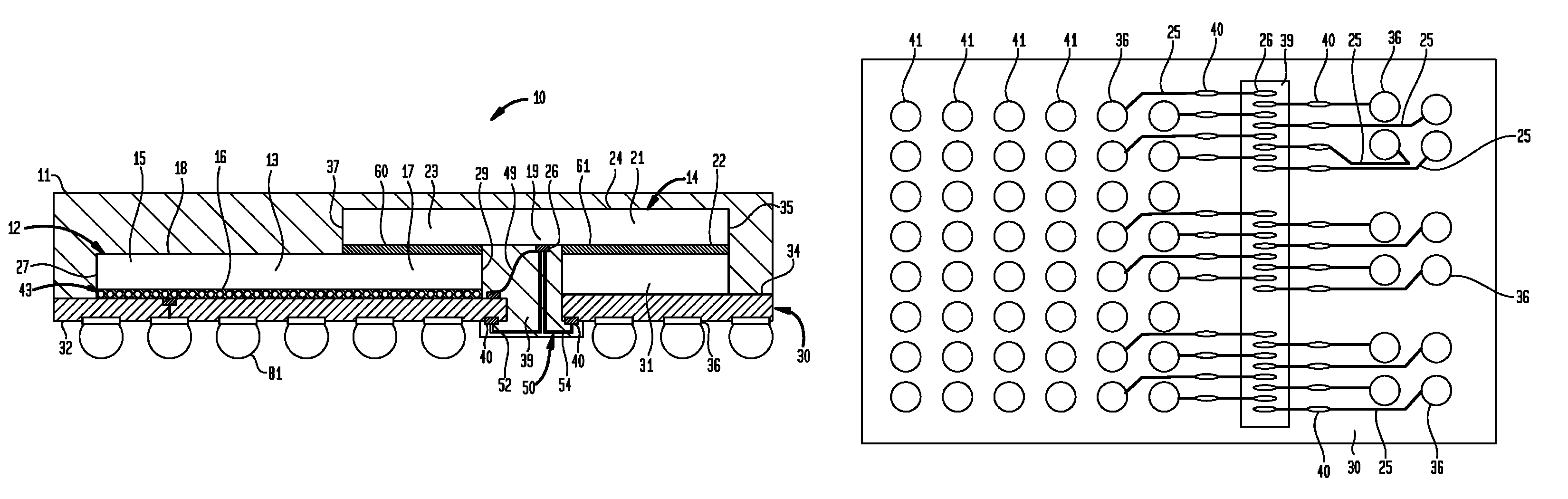
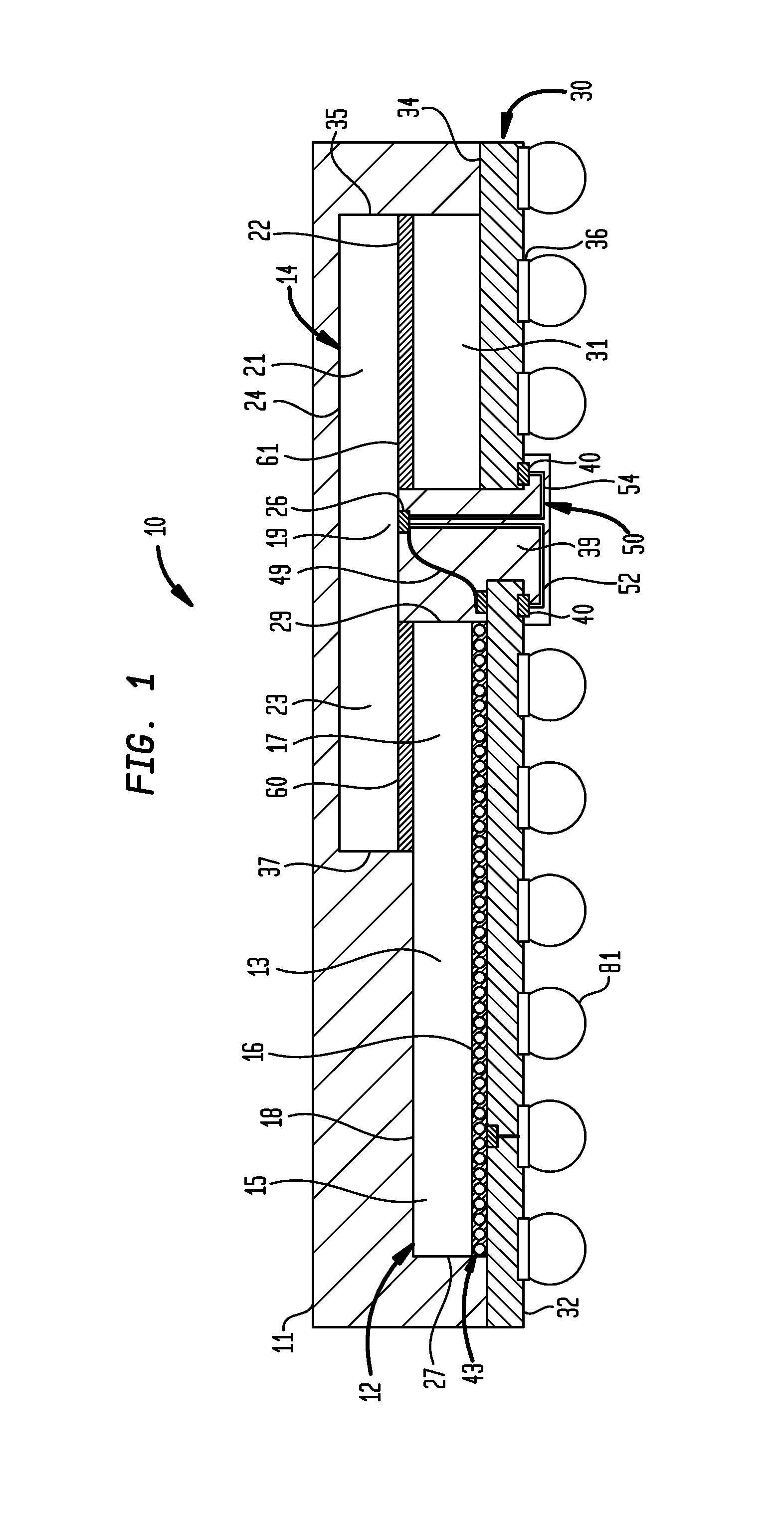
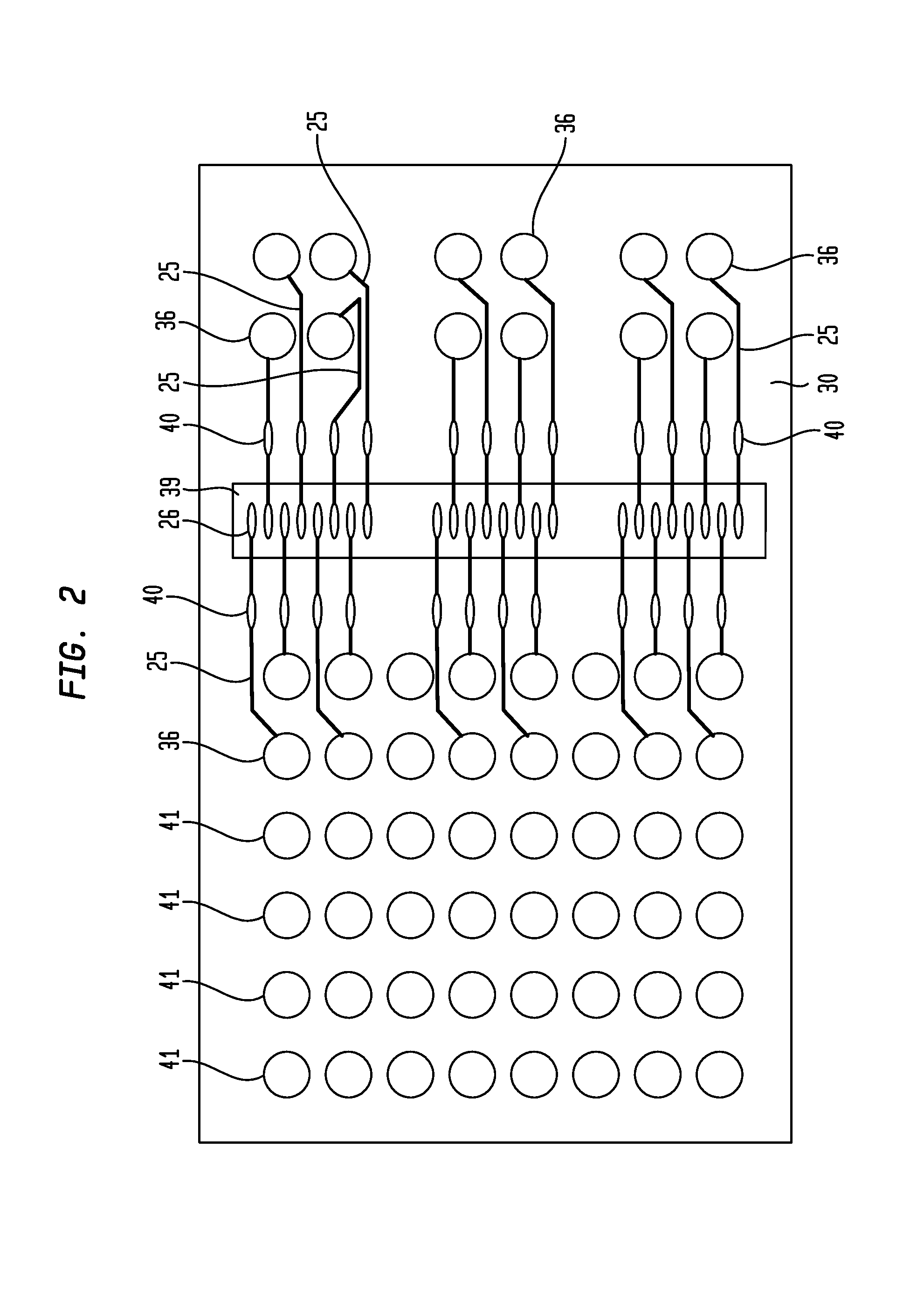
[0028]With reference to FIGS. 1 and 2, a stacked microelectronic assembly 10 according to an embodiment of the present invention includes a first microelectronic element 12 in a face down or flip-chip position and a second microelectronic element 14 in a face down position. In some embodiments, the first and second microelectronic elements 12 and 14 may be a semiconductor chip, or an element including a semiconductor chip, which has contacts at the front surface 16 thereof. The semiconductor chip may be a thin slab of a semiconductor material, such as silicon or gallium arsenide, and may be provided as individual, prepackaged units. The semiconductor chip may embody active circuit elements, e.g., transistors, diodes, among others, or passive circuit elements such as resistors, capacitors or inductors, among others, or a combination of active and passive circuit elements. In an “active” semiconductor chip, the active circuit elements in each microelectronic element typically are elec...


PUM


Abstract

A microelectronic assembly can include a substrate having an aperture extending between first and second surfaces thereof, the substrate having substrate contacts at the first surface and terminals at the second surface. The microelectronic assembly can include a first microelectronic element having a front surface facing the first surface, a second microelectronic element having a front surface facing the first microelectronic element, and leads electrically connecting the contacts of the second microelectronic element with the terminals. The second microelectronic element can have contacts exposed at the front surface thereof beyond an edge of the first microelectronic element. The first microelectronic element can be configured to regenerate at least some signals received by the microelectronic assembly at the terminals and to transmit said signals to the second microelectronic element. The second microelectronic element can embody a greater number of active devices to provide memory storage array function than any other function.

Description

CROSS-REFERENCE TO RELATED APPLICATIONS[0001]The present application claims the benefit of the filing date of U.S. Provisional Patent Application Ser. No. 61 / 477,883, filed Apr. 21, 2011, the disclosure of which is hereby incorporated by reference herein. The following commonly-owned applications are hereby incorporated by reference herein: U.S. Provisional Patent Application Ser. Nos. 61 / 477,820, 61 / 477,877, and 61 / 477,967, all filed Apr. 21, 2011.BACKGROUND OF THE INVENTION[0002]The present invention relates to stacked microelectronic assemblies and methods of making such assemblies, and to components useful in such assemblies.[0003]Semiconductor chips are commonly provided as individual, prepackaged units. A standard chip has a flat, rectangular body with a large front face having contacts connected to the internal circuitry of the chip. Each individual chip typically is mounted in a package which, in turn, is mounted on a circuit panel such as a printed circuit board and which c...

Claims


Application Information

Patent Timeline
Patent Type & Authority Patents(United States)
IPC IPC(8): H01L23/02
CPCH01L23/3128H01L25/0652H01L25/0657H01L25/50H01L25/03H01L25/105H01L25/071H01L2224/16227H01L2224/48227H01L2224/4824H01L2224/73204H01L2224/73253H01L2224/73265H01L2225/06558H01L2225/06562H01L2924/09701H01L2924/1461H01L2924/15311H01L2924/01087H01L2224/32145H01L2224/32225H01L2224/16225H01L2224/16245H01L2224/48247H01L2224/4826H01L2224/73215H01L2924/3011H01L2224/06136H01L2224/0401H01L2224/06135H01L2924/00H01L2924/00012H01L2224/32245H01L2224/48095H01L2924/181H01L24/73H01L25/065H01L25/10H01L23/31H01L21/38
Inventor HABA, BELGACEMCRISP, RICHARD DEWITTZOHNI, WAEL
Owner TESSERA INC
Why Eureka
Try Eureka