Timing control circuit

a timing control and circuit technology, applied in the field of data processing, can solve the problems of large circuit area, high overhead, and difficulty in predicting in advance which timings to use, and achieve the effect of easy understanding

Active Publication Date: 2012-11-06
ARM LTD
View PDF2 Cites 3 Cited by
  • Summary
  • Abstract
  • Description
  • Claims
  • Application Information

AI Technical Summary

Benefits of technology

[0018]As the bits of the control value directly control whether corresponding groups of control units are in an active mode or an inactive mode, there is no need for a decoder for converting the control value into individual signals for switching each control unit. Hence the area overhead associated with a timing control circuit can be reduced. For example, in one embodiment a tunable timing control circuit having 15 control units can be provided with as few as 19 transistors.
[0061]To enable the memory compiler to produce a memory design which can be used for different sizes of memory arrays, the present technique allows the memory compiler to compile a memory having a dummy loop circuit which controls the reference timing according to the present technique. Hence, the reference timings may be adjusted in the eventually implemented memory array. Since the dummy loop circuit has current control units which are switched collectively in groups between active and inactive modes, the area overhead associated with this design of dummy loop circuit is low in comparison to previous systems where each current control unit is switched individually. Hence, the memory compiler is able to produce memory designs having low area overhead.

Problems solved by technology

For example, it may not be easy to predict in advance which timings should be used since the ideal signal timing may vary from system to system depending on the configuration of circuit elements used in the system, manufacturing process variations and other characteristics of the system.
However, providing such variable timing control requires a large amount of circuit area.
This area overhead is expensive and contributes greatly to the total circuit area of the memory.

Method used


Image

  • Timing control circuit
  • Timing control circuit
  • Timing control circuit

Examples


Embodiment Construction

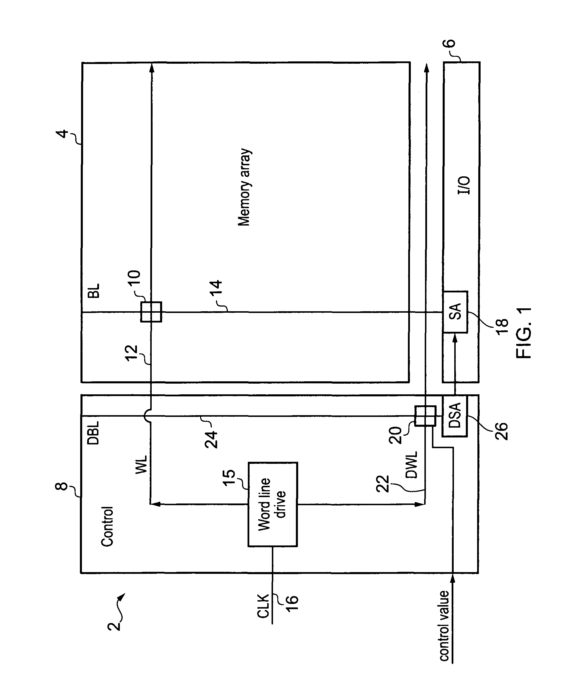
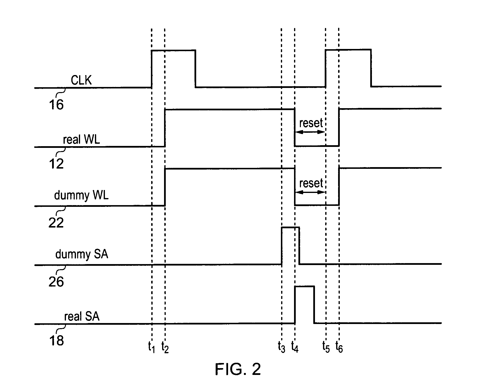
[0088]FIG. 1 schematically illustrates a memory 2 comprising a memory array 4, an input / output (I / O) unit 6 and a control unit 8. The memory array 4 comprises an array of memory cells 10 for storing data values. Each memory cell 10 has a corresponding word line 12 and bit line 14 which are used to select the desired memory cell 10 during a read operation or write operation. During a read or write operation, the word line 12 for the desired memory cell 10 is driven by a word line drive unit 15 within the control unit 8 in response to a clock signal 16. For a read operation, the data value in the memory cell 10 is read from the bit line 14 by a sense amplifier 18 within the input / output unit 6. For a write operation, a data value is asserted on the bit line 14 and stored to the memory cell 10.

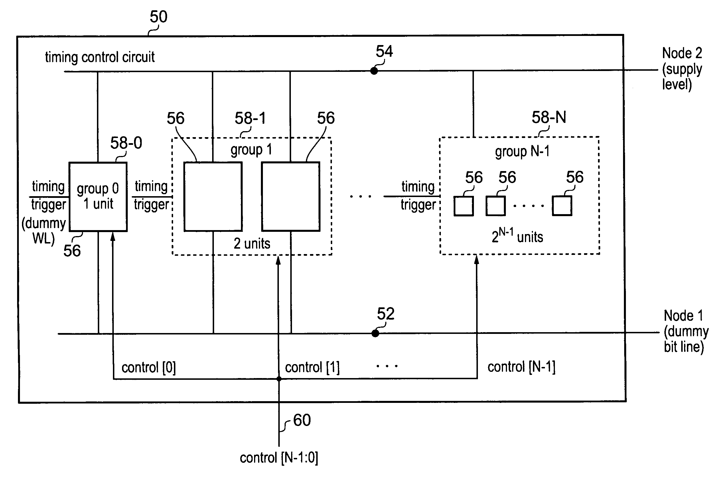
[0089]Reference timings for controlling memory operations within the memory array 4 are controlled by a dummy loop circuit. The dummy loop circuit comprises a dummy cell 20, dummy word line 22, d...


PUM


Abstract

A timing control circuit comprises at least three current control units coupled in parallel between a first circuit and a second circuit node. The current control units each have an active mode and an inactive mode. The current control units are responsive to a timing trigger event to pass current whose magnitude is dependent on how many of the current control units are in the active mode. The current control units comprise a plurality of groups. Current control units within a same group are responsive to a change in a bit of a control value corresponding to that group to switch together between the active and inactive modes, such that the magnitude of the current is dependent on which of the groups are in the active mode. The signal timing in the associated circuit is varied in dependence on the magnitude of the current.

Description

BACKGROUND OF THE INVENTION[0001]1. Field of the Invention[0002]The present invention relates to the field of data processing. More particularly, the invention relates to a timing control circuit for controlling a signal timing in an associated circuit.[0003]2. Description of the Prior Art[0004]In a data processing system, it can be useful to control a signal timing within a circuit of the data processing system. For example, it may not be easy to predict in advance which timings should be used since the ideal signal timing may vary from system to system depending on the configuration of circuit elements used in the system, manufacturing process variations and other characteristics of the system. Also, it may be desirable to provide reference timings that can varied in accordance with application requirements. For example, a more aggressive scheduling with a shorter delay between reference timings can increase performance, while for a safety-critical application the timings can be r...

Claims


Application Information

Patent Timeline
Patent Type & Authority Patents(United States)
IPC IPC(8): G11C7/22G06F1/04G06F7/22
CPCG11C7/08G11C7/14G11C7/22G11C11/413
Inventor VAN WINKELHOFF, NICOLAAS KLARINUS JOHANNESAGHETTI, BASTIEN JEAN CLAUDE
Owner ARM LTD
Why Eureka
Try Eureka