
Active matrix substrate, liquid crystal panel, display, television receiver

a technology of active matrix and liquid crystal board, applied in non-linear optics, instruments, optics, etc., can solve the problem of more likely formation of defective contact holes, and achieve the effect of high precision and high precision

Active Publication Date: 2012-12-11
SHARP KK
View PDF47 Cites 8 Cited by
  • Summary
  • Abstract
  • Description
  • Claims
  • Application Information

AI Technical Summary

Benefits of technology

The present invention aims to provide an active matrix substrate in which two wirings are connected with high precision, and a short circuit between them is prevented. The invention includes a non-display region with a reduced thickness insulating film that includes a through-bore portion and a portion with a reduced thickness adjacent to the through-bore portion. The insulating film is formed by boring through a part of the insulating film that has a large thickness at the location where the contact hole is to be formed. This arrangement ensures that the trunk wiring and the storage capacitor wiring are connected with high precision, while a short circuit between them is prevented. Additionally, the invention includes an active matrix substrate with individual control of electric potentials supplied to the first and second storage capacitor wirings, which allows one pixel area to have a plurality of subregions with different luminances.

Problems solved by technology

Further, the same problem as above concerns the portion of the insulating film 803 in the non-display region at which portion each of the scanning signal lines is to be connected, via a contact hole, with a lead wiring for external connection.
In this case, a defective contact hole is more likely to be formed due to variation and the like in thickness and quality of the insulating film.

Method used


Image

  • Active matrix substrate, liquid crystal panel, display, television receiver
  • Active matrix substrate, liquid crystal panel, display, television receiver
  • Active matrix substrate, liquid crystal panel, display, television receiver

Examples


Embodiment Construction

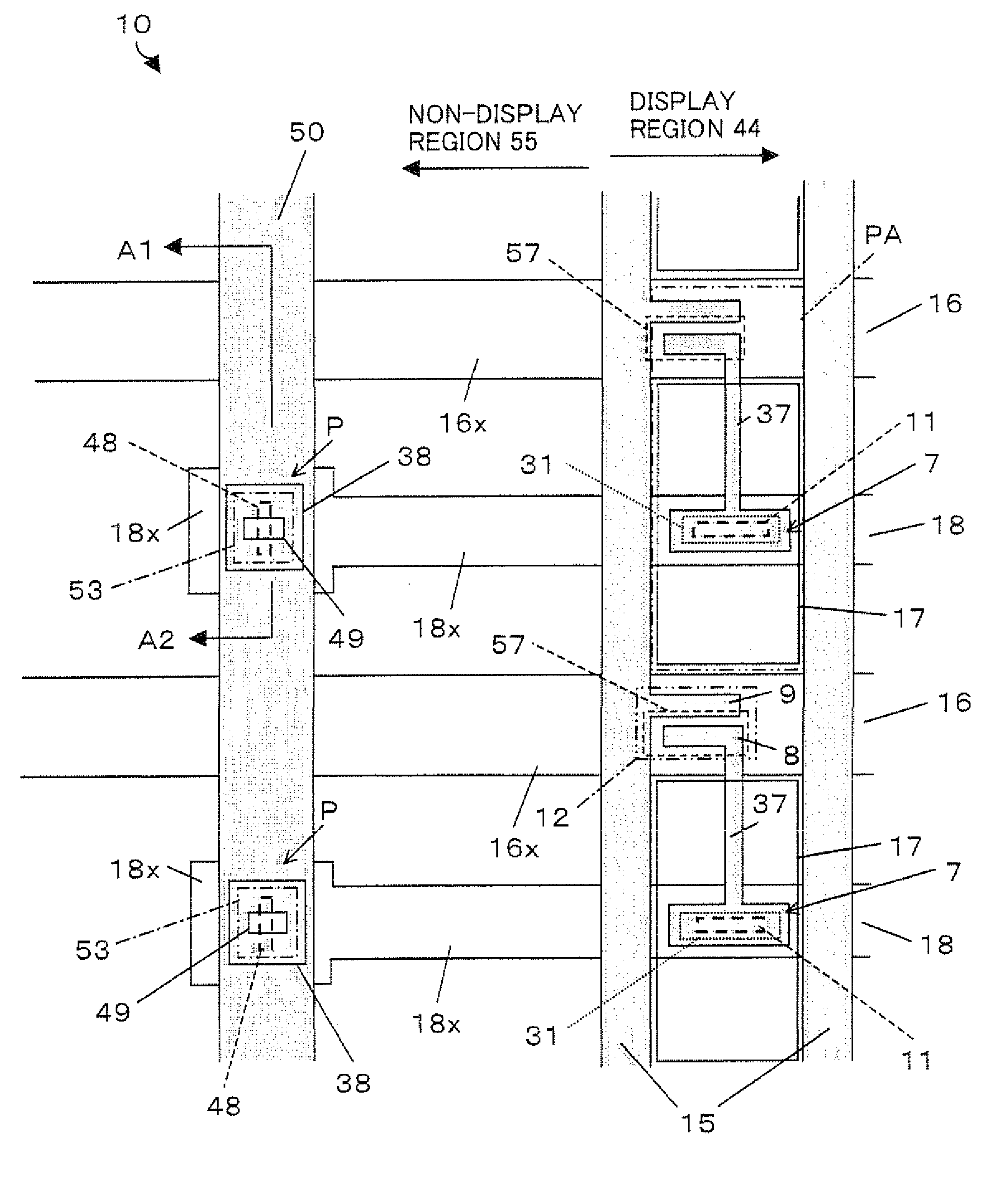
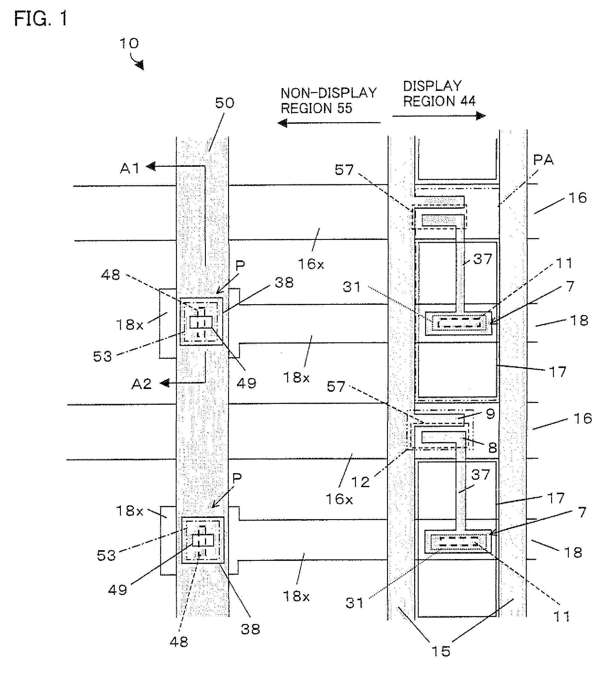
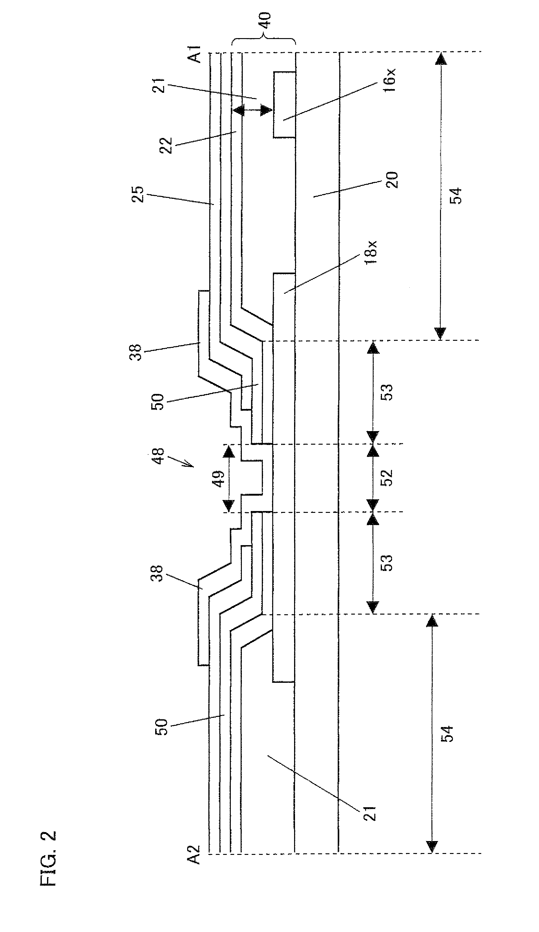
[0114]The following description deals with Embodiment 1 of the present invention with reference to FIGS. 1 through 36. FIG. 1 is a plan view schematically showing the structure of an active matrix substrate (display region, non-display region) of the present embodiment. FIG. 2 is a cross-sectional view taken along arrows A1-A2 shown in FIG. 1.

[0115]As shown in FIG. 1, an active matrix substrate 10 includes in its display region 44: a scanning signal line 16 formed in the horizontal direction in the figure; a data signal line 15 formed in the vertical direction in the figure, the scanning signal line 16 and the data signal line 15 crossing each other at right angle; a thin film transistor (TFT) 12 formed adjacent to the intersections of the signal lines (15, 16); a pixel electrode 17; and a storage capacitor wiring (Cs wiring) 18 formed in the horizontal direction in the figure. Hereinafter, the horizontal direction in the figure refers to a direction along the scanning signal line o...


PUM

PropertyMeasurementUnit
thicknessaaaaaaaaaa
thicknessaaaaaaaaaa
thicknessaaaaaaaaaa

Abstract

An active matrix substrate includes: storage capacitor wirings (18); a Cs trunk wiring (50) connected with the storage capacitor wirings via contact holes (48) provided in a non-display region (44); scanning signal lines (16) provided in the same layer as the storage capacitor wirings (18) and crossing the Cs trunk wiring (50) in the non-display region (44); an insulating layer between the storage capacitor wirings (18) and the Cs trunk wiring (50) which includes: a through-bore portion for forming the contact hole (48); a first film thickness portion (53) adjacent to the through-bore portion; and a second film thickness portion which is thicker than the first film thickness portion (53) and situated at least in the intersections of the storage capacitor wirings (18) with the Cs trunk wiring (50). Consequently, the storage capacitor wirings (18) and the Cs trunk wiring (50) are connected with high precision, and a short circuit between the Cs trunk wiring (50) and the scanning signal lines (16) is unlikely to occur.

Description

[0001]This application is the U.S. national phase of International Application No. PCT / JP2007 / 057049 filed, 30 Mar. 2007 which designated the U.S. and claims priority to Japanese Application No(s) 2006-197319 filed 19 Jul. 2006 and 2006-332592, filed 8 Dec. 2006, the entire contents of each of which are hereby incorporated by reference.TECHNICAL FIELD[0002]The present invention relates to display devices such as liquid crystal display devices and various types of EL display devices, and to active matrix substrates for use in such display devices.BACKGROUND ART[0003]Active matrix substrates are widely used in active matrix display devices such as liquid crystal display devices and electro luminescence (EL) display devices. A normal active matrix substrate includes, in its display region: scanning signal lines; data signal lines; and thin film transistors (TFTs) provided at the intersections of those signal lines. Electric potential signals are transmitted as appropriate from the data...

Claims


Application Information

Patent Timeline
Patent Type & Authority Patents(United States)
IPC IPC(8): G02F1/1333G02F1/1339G02F1/1343
CPCG02F1/1345G02F1/13458G02F1/136286
Inventor TSUBATA, TOSHIHIDEYAGI, TOSHIFUMI
Owner SHARP KK
Learn More