Active array substrate for flat panel display

a flat panel display and active array technology, applied in non-linear optics, instruments, optics, etc., can solve problems such as abnormal frames, reduce the resistance of the “repair circuit” of the active array substrate, and reduce the probability of the phenomenon of weak line resulting from heavier load

Active Publication Date: 2012-12-11
AU OPTRONICS CORP
View PDF12 Cites 0 Cited by
  • Summary
  • Abstract
  • Description
  • Claims
  • Application Information

AI Technical Summary

Benefits of technology

[0010]Therefore, the active array substrate of the FPD of the invention is capable of solving the problem of the phenomenon of abnormal pixel display resulting from the data lines having breaches by using a “repair circuit” constituted by the first repair lines, the second repair lines and the third repair lines. After the repair procedure, the signals from the data driver chips can be transmitted to the thin film transistors of the pixels beneath the breach through the “repair circuit” such that the pixels can be controlled by the data driver chips to operate normally. In addition, since the widths of the intersection of the first repair lines and the data lines are smaller than the widths of other parts of the first repair lines. The widths of the intersection of the second repair lines and the data lines are smaller than the widths of other parts of the second repair lines. In the “repair circuit”, the capacitance caused by the intersection of the first repair lines and the data lines and by the intersection of the second repair lines and the data lines can be reduced, thereby the loading in operation of the “repair circuit” of the active array substrate of the FPD of the invention can be decreased.
[0011]Moreover, since the third repair lines of the active array substrate of the FPD of the present invention has a double layered conductive structure to be a parallel circuit with a plurality of conductive units, the resistance of the “repair circuit” of the active array substrate of the FPD of the invention can be further reduced. Hence, in the active substrate of the FPD of the present invention, the “repair circuit” constituted by the first repair lines, second repair lines and third repair lines has a conductive resistance significantly lower than that of the conventional “repair circuit” such that the probability of the “weak line” phenomenon resulting from heavier load is reduced and the flat panel display provided with the active array substrate of the present invention can display normally after the repair procedure.

Problems solved by technology

It results in an abnormal frame, and the phenomenon is called “weak line”.

Method used


Image

  • Active array substrate for flat panel display
  • Active array substrate for flat panel display
  • Active array substrate for flat panel display

Examples


Embodiment Construction

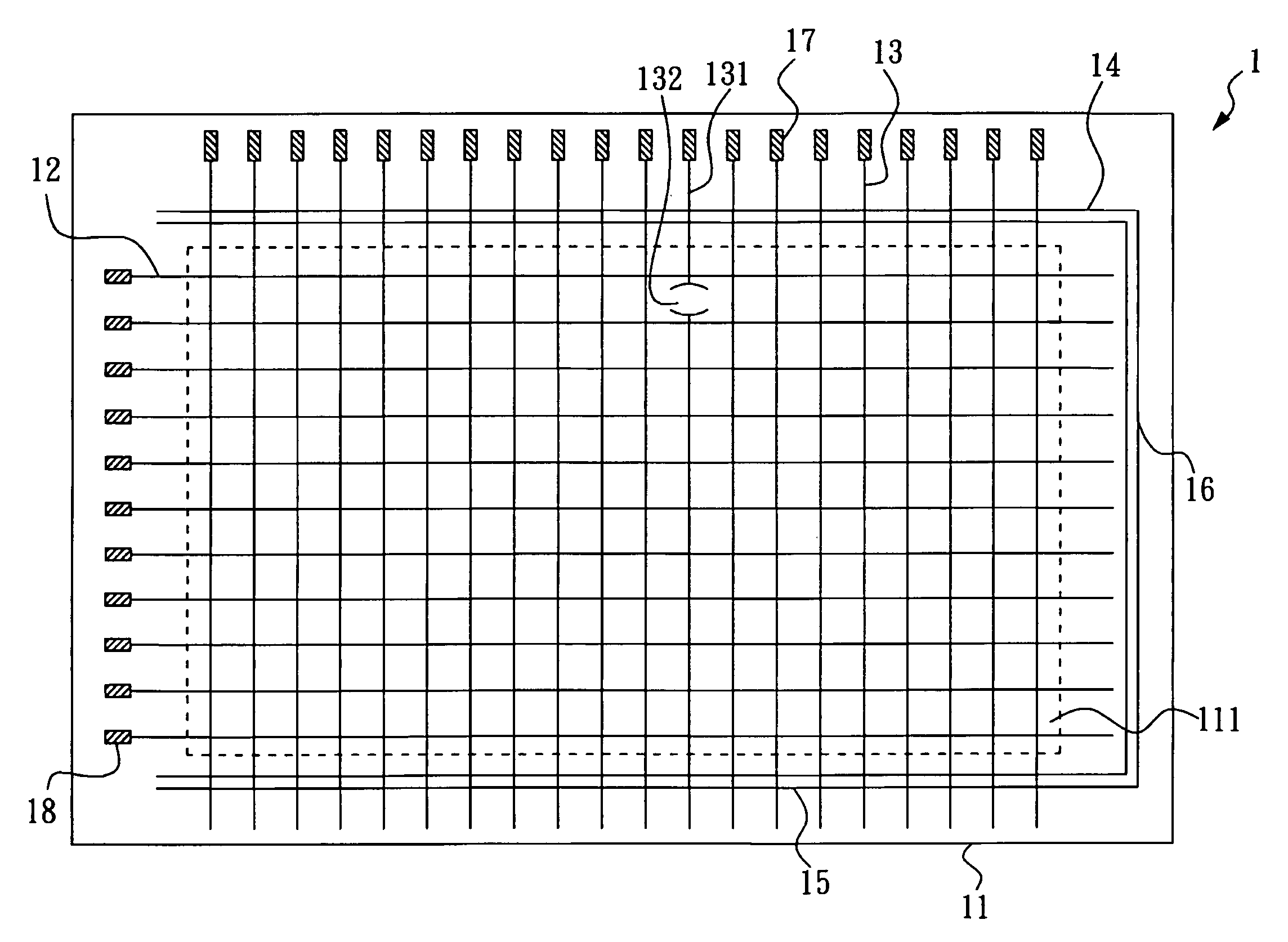
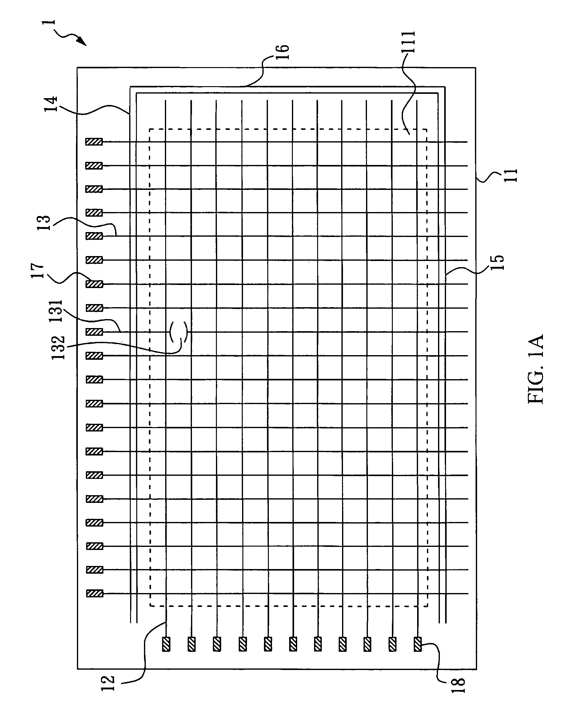
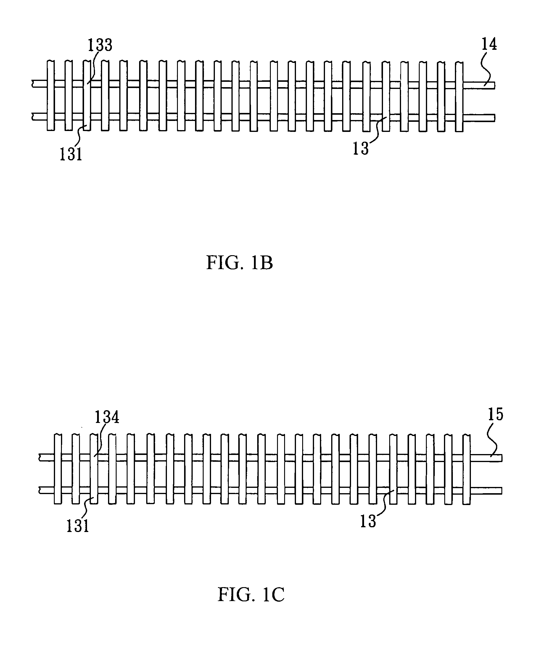
[0030]FIG. 2A is a schematic diagram of an active array substrate for the FPD of the first preferred embodiment of the invention. An active array substrate 2 of the FPD of the first preferred embodiment of the invention includes a substrate 21, a plurality of scanning lines 22, a plurality of data lines 23, a plurality of first repair lines 24, a plurality of second repair lines 25, and a plurality of third repair lines 26. The substrate 21 has a display area 211. The plurality of scanning lines 22 and the plurality of data lines 23 are disposed on the substrate 21, and they cross but not in electrical connection with each other in the display area 211. On the other hand, the plurality of first repair lines 24 and the plurality of second repair lines 25 are disposed on the substrate 21. The plurality of first repair lines 24 and the plurality of second repair lines 25 respectively cross with the plurality of data lines 23 at the upper area and the lower area outside the display area...


PUM

PropertyMeasurementUnit
areaaaaaaaaaaa
conductiveaaaaaaaaaa
widthsaaaaaaaaaa

Abstract

An active array substrate for a flat panel display is disclosed. The active array substrate includes a substrate, a plurality of first conductive lines, a plurality of second conductive lines, a plurality of first repair lines, a plurality of second repair lines, a plurality of third repair lines. The substrate has a display area. The first repair lines cross and are electrically separated from the second conductive lines. The second repair lines cross and are electrically separated from the second conductive lines. Each of the third repair lines is in electrical connection respectively with one of the first repair lines and one of the second repair lines. The second conductive lines are divided into a plurality of second conductive line groups and each of the second conductive line groups respectively corresponds to one of the third repair lines.

Description

BACKGROUND OF THE INVENTION[0001]1. Field of the invention[0002]This invention relates to an active array substrate for a flat panel display (FPD), particularly to an active array substrate for a liquid crystal display, and is capable of lowering the probability of the phenomenon of “weak line” resulting from heavier load of a repair circuit.[0003]2. Description of Related Art[0004]FIG. 1A shows a schematic diagram of an active array substrate for a conventional flat panel display. As shown in FIG. 1A, a conventional active array substrate 1 includes a substrate 11, a plurality of scanning lines 12, a plurality of data lines 13, a plurality of first repair lines 14, a plurality of second repair lines 15, and a plurality of third repair lines 16. The substrate 11 has a display area 111. The scanning lines 12 and the data lines 13 are disposed on the substrate 11. In the display area 111, the scanning lines 12 and the data lines 13 are crossed and electrically separated from each othe...

Claims


Application Information

Patent Timeline
Patent Type & Authority Patents(United States)
IPC IPC(8): G02F1/13G02F1/1333G02F1/1343
CPCG02F1/136259
Inventor SHIAO, TSUNG-JIEHHUANG, TIEN-CHUNLIU, SHOU-LIE
Owner AU OPTRONICS CORP
Why Eureka
Try Eureka