Boolean satisfiability based verification of analog circuits

a verification process and logic technology, applied in the field of formal verification of systems, can solve the problems of increasing design challenges, and wasting time and money on verification processes of the general type described above, and achieving the effect of reducing design complexity and time-consuming and labor-intensive problems

Inactive Publication Date: 2012-12-25
CADENCE DESIGN SYST INC
View PDF2 Cites 7 Cited by
  • Summary
  • Abstract
  • Description
  • Claims
  • Application Information

AI Technical Summary

Benefits of technology

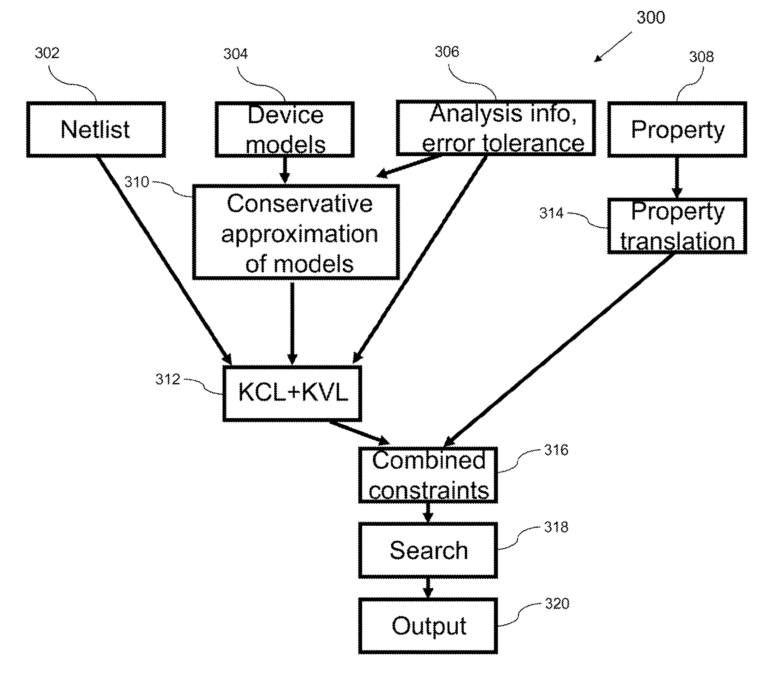
[0012]In one aspect of the invention, a method is provided to formally verify a property of a circuit design. A description of at least a portion of the circuit and a description of a relationship between current and voltage (I-V relationship) for one or more devices in the circuit are used to produce conservative approximations for device I-V behavior. Voltage labels are assigned to one or more terminals of one or more of the devices that indicate voltage relationships among the one or more terminals consistent with KVL. Current relationship among one or more respective sets of curr

Problems solved by technology

Aggressive scaling down of device dimensions due to advances in semiconductor manufacturing technologies has made these designs ever more challenging as designers need to ensure that the circuit works over wide ranges of process, voltage and temperature (PVT) conditions.
The verification process of the general type described above is a very time consuming methodology with no guarantees that the circuit will work in all possible simulation scenarios that have not been tested.
As a result, experienced analog circuit designers often spend a significant portion of their time designing basic circuit blocks and porting them from one technology node to another.
As newer, aggressive manufacturing processes were developed, the problem of designing a circuit became more challenging.
Thus, the circuit simulation problem has transformed into a verification problem wherein the designer is looking for some “guarantee

Method used


Image

  • Boolean satisfiability based verification of analog circuits
  • Boolean satisfiability based verification of analog circuits
  • Boolean satisfiability based verification of analog circuits

Examples


example

Resistor-Diode Circuit

[0058]FIG. 4 is an illustrative drawing of a circuit that includes a resistor and a diode-connected transistor (hereinafter diode), which may be a portion of a larger circuit (not shown). The circuit includes a shared connection 501 / 503 between a terminal 501 of the transistor and a terminal 503 of the resistor associated with voltage V and current I as shown. A Vdd bias voltage is coupled to a terminal 504 of the resistor, and an effective ground voltage is coupled to a terminal 506 of the diode.

[0059]FIG. 5 is an illustrative drawing of showing separately the diode and the resistor of FIG. 4 and showing their associated currents and voltages. The diode has terminals 501 and 506. Diode voltage Vg is across diode terminals 501 and 506. A diode current Id flows through the diode from terminal 501 to terminal 506. The resistor has terminals 504 and 503. A voltage Vdd is associated with resistor terminal 504, and a voltage Vr is associated with resistor terminal 5...


PUM


Abstract

A method is provided to formally verify a property of a circuit design comprising: receiving a description of at least a portion of the circuit; receiving an indication of search accuracy criteria; receiving a description of a relationship between current and voltage (I-V relationship) for one or more of devices of the circuit; converting each I-V relationship to a conservative approximation of such I-V relationship; assigning voltage labels to one or more terminals of one or more identified devices that indicate voltage relationships among the one or more terminals consistent with KVL; defining a respective current relationship among one or more respective sets of currents of the one or more of the identified devices that is consistent with KCL; searching for one or more combinations of current and voltage values that are within at least one region of each conservative approximation and that are consistent with the voltage labels and that are consistent with each respective defined current relationship; converting each region determined to have a searched for combination of current and voltage values to multiple respective smaller regions; and repeating the acts of searching and converting until regions are obtained that meet the received search accuracy criteria.

Description

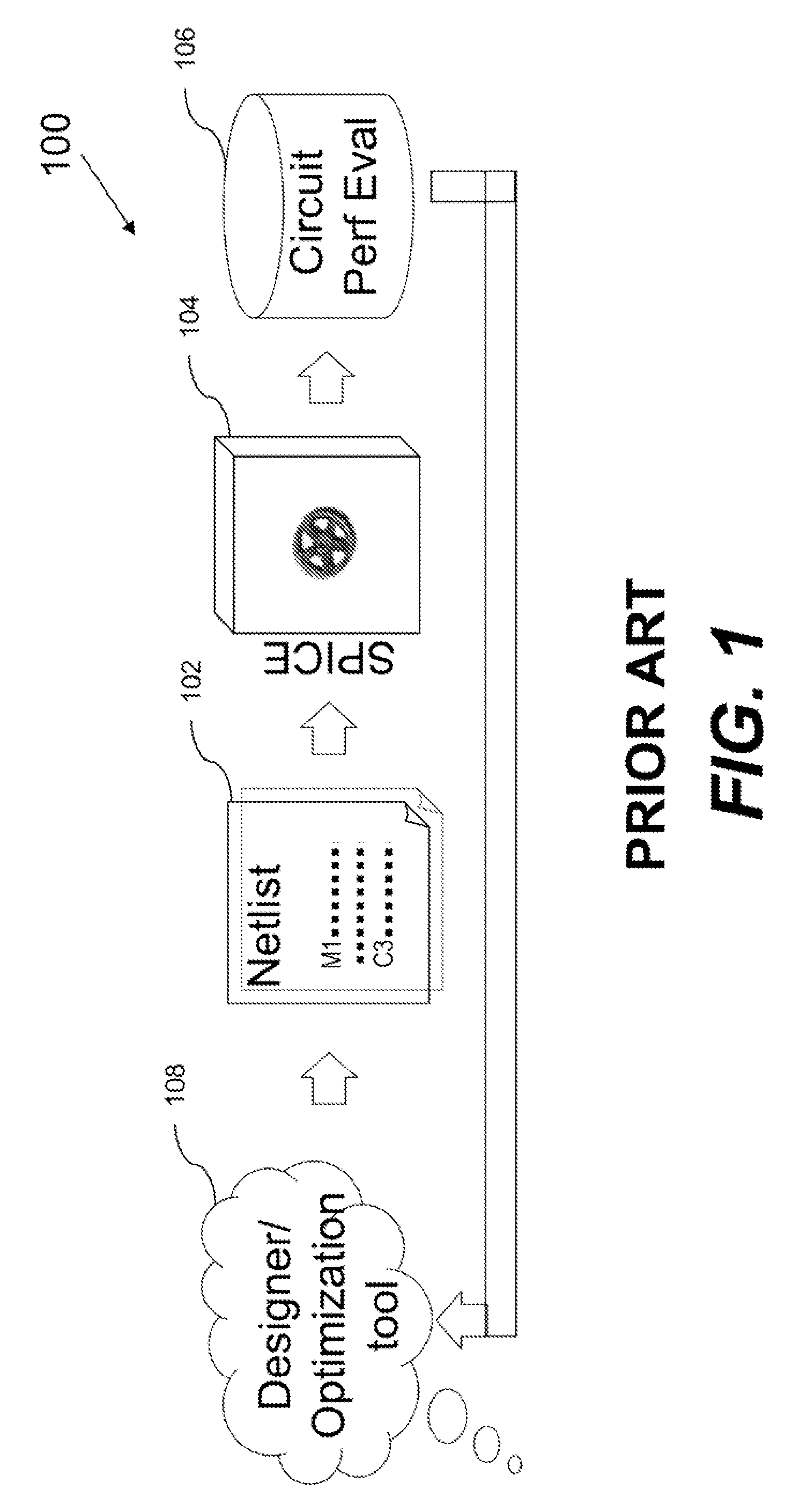
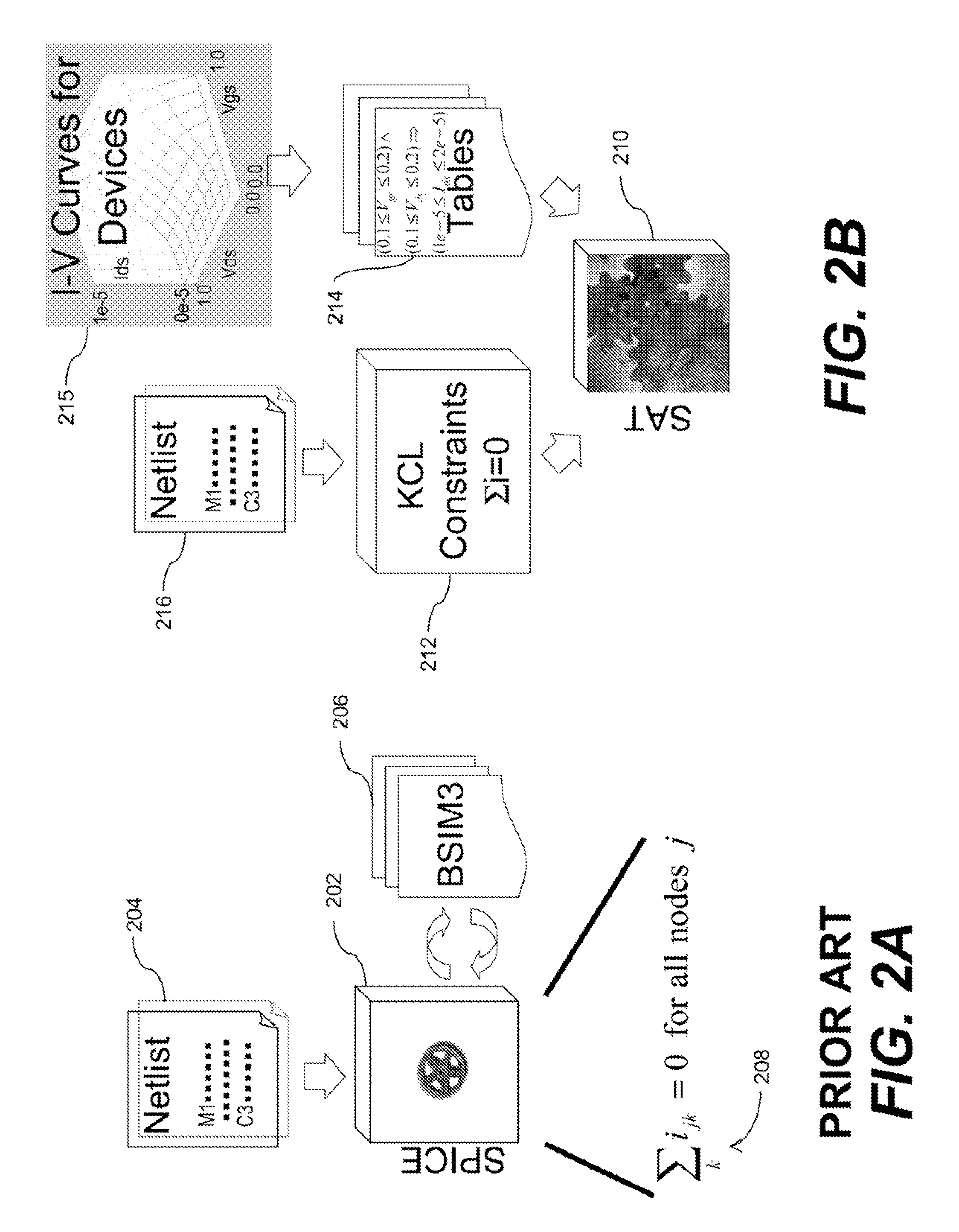
BACKGROUND OF THE INVENTION[0001]1. Field of the Invention[0002]The invention relates in general to formal verification of a system, and more particularly, to verification of analog circuits.[0003]2. Description of the Related Art[0004]FIG. 1 is an illustrative drawing of flow of a typical analog circuit verification process. SPICE remains the tool of choice for analog circuit designers. The most common way of verifying analog circuits has been to run a sequence of SPICE simulations and post processing the simulation results to find if the circuit fails to meet the specifications for any of the sampled cases. Once the failing cases have been identified, the design is tweaked and the simulations redone. This process is repeated until the circuit passes all the tests. More specifically, referring to FIG. 1, a verification process 100 typically involves a loop in which a circuit netlist 102 for a design that identifies devices and nets interconnecting the devices is input to an analog ...

Claims


Application Information

Patent Timeline
IPC IPC(8): G06F9/455G06F17/50
CPCG06F17/5036G06F17/504G06F30/3323G06F30/367
Inventor TIWARY, SAURABH K.GUPTA, ANUBHAVPHILLIPS, JOEL R.PINELLO, CLAUDIOZLATANOVICI, RADU
Owner CADENCE DESIGN SYST INC
Why Eureka
Try Eureka