Light emitting element

a technology of light-emitting elements and light-emitting components, which is applied in the direction of basic electric elements, electrical equipment, and semiconductor devices, can solve the problems of limitation of light-emitting output enhancement and inability to increase light-emitting output, and achieve the effect of increasing the thickness of the reflecting layer and enhancing the light-emitting outpu

Inactive Publication Date: 2013-01-08
SUMITOMO CHEM CO LTD
View PDF3 Cites 4 Cited by
  • Summary
  • Abstract
  • Description
  • Claims
  • Application Information

AI Technical Summary

Benefits of technology

[0028]According to the invention, a light emitting element that is capable of enhancing a light emission output in accordance with increase in thickness of a reflecting layer, even if the reflecting layer has a thickness of not less than a predetermined value.

Problems solved by technology

However, although the light emitting element disclosed in the JP-A-5-37017 is capable of broadening reflection wavelength region in a single body of the light reflection layer, if the light reflection layer has a thickness of not less than a predetermined value, the light emission output can not be increased, similarly to a case of using a light reflection layer that does not have the chirp-like shape.
Namely, if the thickness of the light reflection layer becomes not less than 2 μm, enhancement of the light emission output is saturated in the light emitting element disclosed in the JP-A-5-37017, and there is a limitation to the enhancement of the light emission output.

Method used


Image

  • Light emitting element
  • Light emitting element
  • Light emitting element

Examples


first embodiment

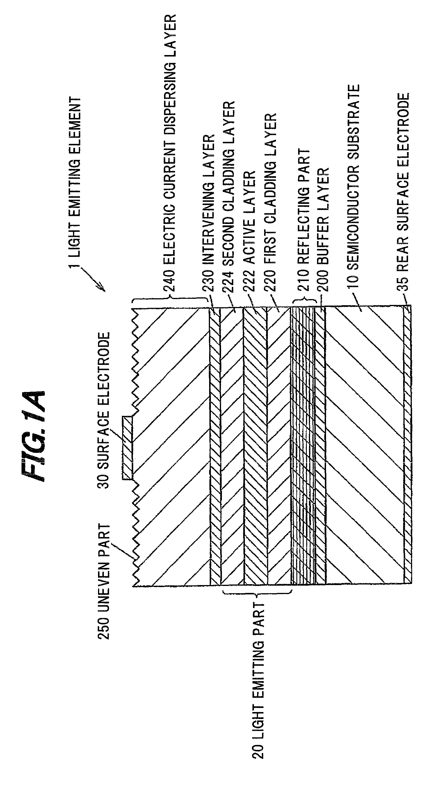
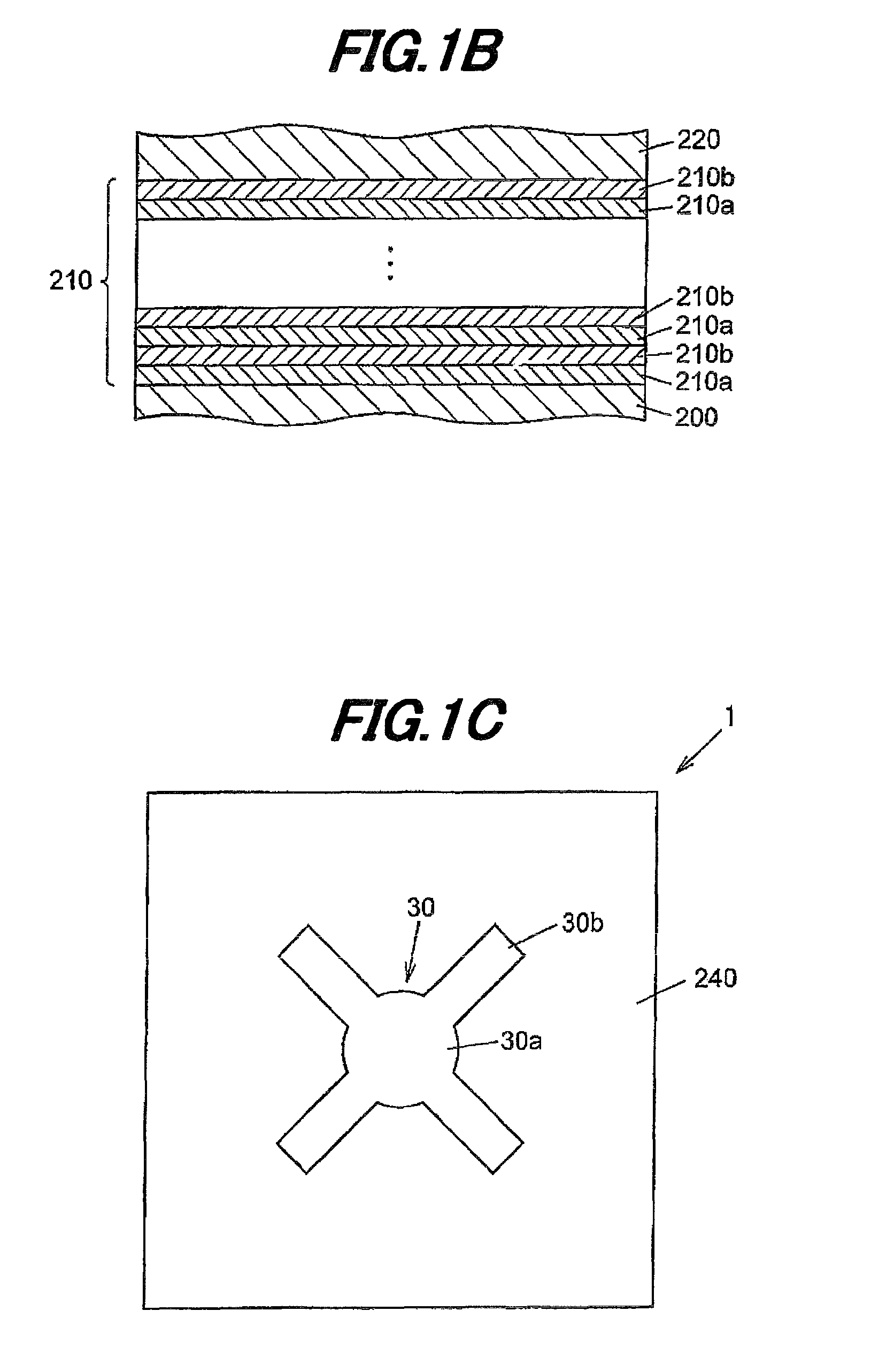
[0047]FIG. 1A is a cross-sectional view schematically showing a light emitting element according to a first embodiment of the invention, and FIG. 1B is a cross-sectional view schematically showing a reflecting part included in the light emitting element according to the first embodiment of the invention. Further, FIG. 1C is a plan view schematically showing a light emitting element according to a first embodiment of the invention.

[0048]Structural Outline of Light Emitting Element 1

[0049]The light emitting element 1 is, as an example, a light emitting diode (LED) for emitting a red light having peak wavelength (λP) adjacent to 631 nm. Particularly, the light emitting element 1 includes an n-type as a first conductivity type semiconductor substrate 10, an n-type buffer layer 200 disposed on the semiconductor substrate 10, a reflecting part 210 disposed on the buffer layer 200 so as to have a laminated structure of an n-type compound semiconductor, an n-type first cladding layer 220 di...

second embodiment

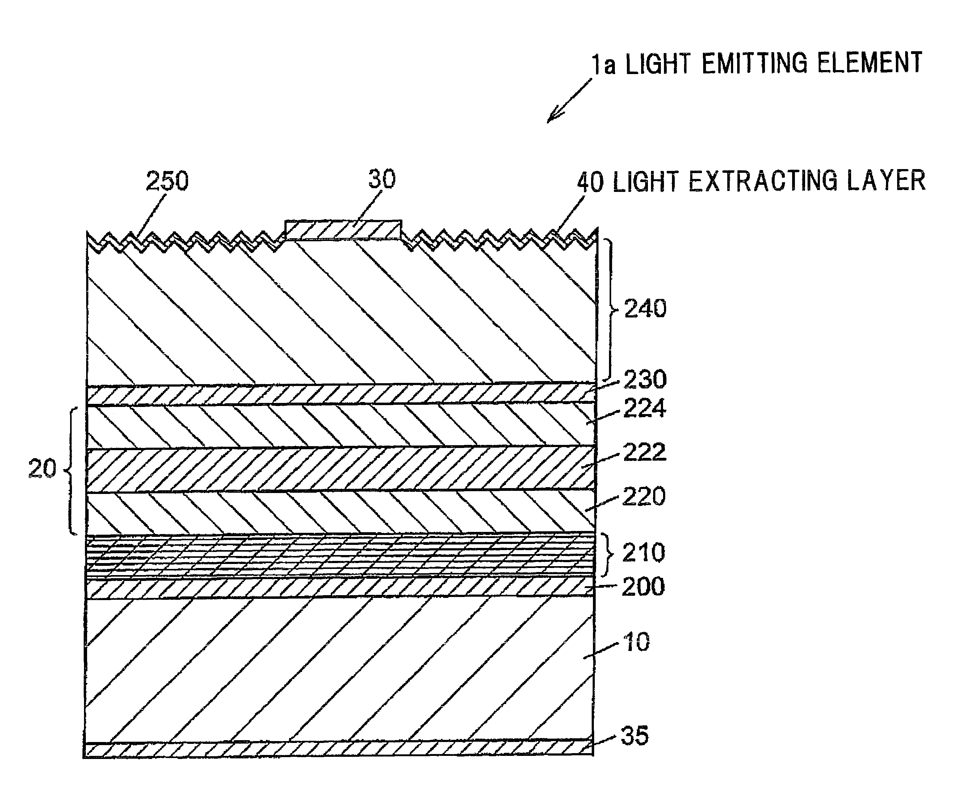
[0091]FIG. 2 is a cross-sectional view schematically showing a light emitting element according to a second embodiment of the invention.

[0092]The light emitting element 1a according to the second embodiment includes almost the same composition as the light emitting element 1 according to the first embodiment except for further including a light extracting layer 40 on the uneven part 250, difference from the light emitting element 1 according to the first embodiment. Therefore, detail explanation will be omitted except for the different points.

[0093]The light emitting element 1a includes the light extracting layer 40 formed on the surface of the electric current dispersing layer 240 except for a region where the surface electrode 30 is formed so as to be formed of a material being transparent to the light emitted from the active layer 222 and having refractive index at the level intermediate between the semiconductor constituting the electric current dispersing layer 240 and air. The...

third embodiment

[0096]FIG. 3 is a cross-sectional view schematically showing a light emitting element according to a third embodiment of the invention.

[0097]The light emitting element 1b according to the third embodiment includes almost the same composition as the light emitting element 1 according to the first embodiment except that the active layer 222 is sandwiched between a first undoped layer 221 and a second undoped layer 223, difference from the light emitting element 1 according to the first embodiment. Therefore, detail explanation will be omitted except for the different points.

[0098]Particularly, the light emitting element 1b according to the third embodiment includes the semiconductor substrate 10, the buffer layer 200 disposed on the semiconductor substrate 10, the reflecting part 210 disposed on the buffer layer 200, a first cladding layer 220 disposed on the reflecting part 210, the first undoped layer 221 disposed on the first cladding layer 220, the active layer 222 disposed on the...


PUM


Abstract

A light emitting element includes a semiconductor substrate, a light emitting part having a first and second conductivity type cladding layers and an active layer sandwiched between the cladding layers. A reflecting part is disposed between the substrate and the light emitting part. A current dispersing layer disposed on a side of the light emitting part opposite to the reflecting. The reflecting part has at least three pair layers of first and second semiconductor layers, the first semiconductor layer has a first thickness, the second semiconductor layer has a second thickness and a plurality of pair layers of the reflecting part have a different thickness to each other as values of the incident angle of light are different with respect to each pair layer. At least one pair layer is defined by the incident angle of light being not less than 50 degrees.

Description

[0001]The present application is based on Japanese patent application No. 2009-231157 filed on Oct. 5, 2009, the entire contents of which are incorporated herein by reference.BACKGROUND OF THE INVENTION[0002]1. Field of the Invention[0003]This invention relates to a light emitting element. In particular, this invention relates to a light emitting element including a semiconductor substrate opaque to a light emitted from an active layer and a reflecting part disposed between the semiconductor substrate and the active layer so as to have a thickness of not less than a predetermined value.[0004]2. Description of the Related Art[0005]Conventionally, a light emitting element is known that includes an n-type GaAs substrate, a light reflection layer disposed on the n-type GaAs substrate, an n-type Al0.45Ga0.55As cladding layer disposed on the light reflection layer, a p-type GaAs active layer disposed on the n-type Al0.45Ga0.55As cladding layer, a p-type Al0.45Ga0.55As cladding layer dispo...

Claims


Application Information

Patent Timeline
Patent Type & Authority Patents(United States)
IPC IPC(8): H01L33/00
CPCH01L33/10H01L33/14
Inventor KONNO, TAICHIROO
Owner SUMITOMO CHEM CO LTD
Why Eureka
Try Eureka