
Stress enhanced junction engineering for latchup SCR

Active Publication Date: 2013-02-19
IBM CORP
View PDF10 Cites 1 Cited by
  • Summary
  • Abstract
  • Description
  • Claims
  • Application Information

AI Technical Summary

Benefits of technology

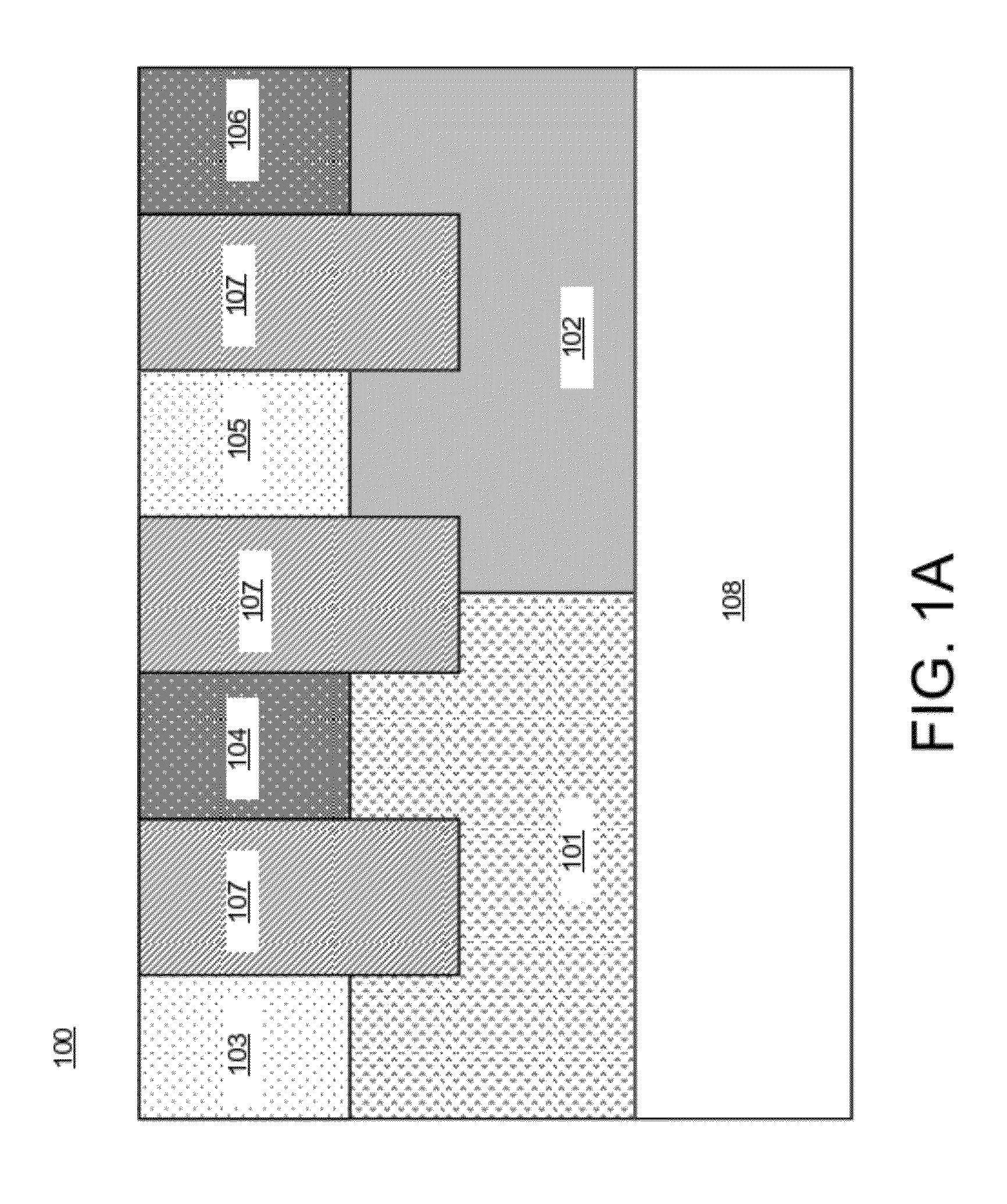
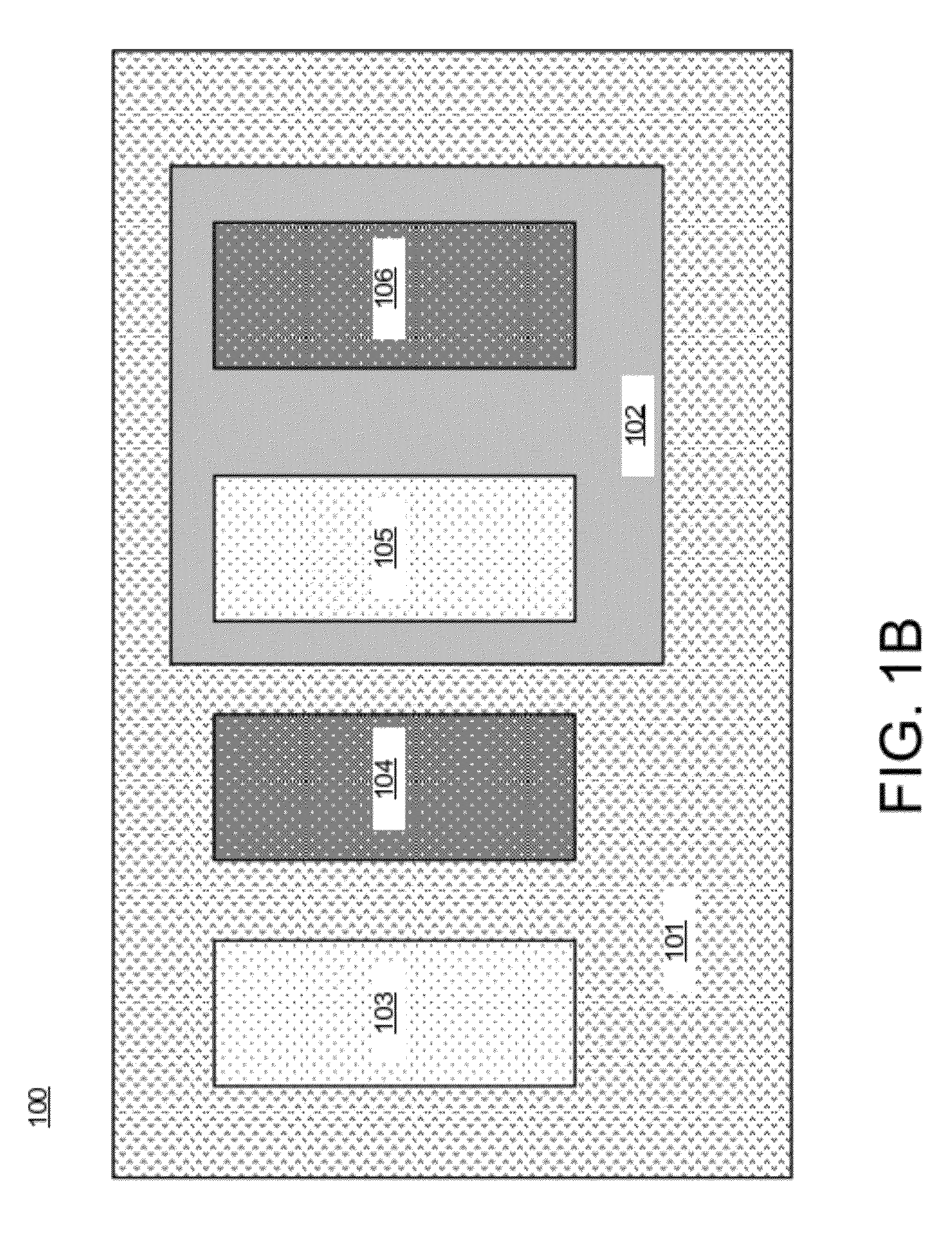
The patent describes a method and device for making an integrated circuit (IC) that includes a latchup silicon controlled rectifier (SCR) and an electrostatic discharge (ESD) SCR. The method involves forming a mask on the substrate, etching the exposed substrate, and selectively depositing a stress engineered junction of the latchup SCR in the etched area. The device includes both the latchup SCR and the ESD SCR, with the ESD SCR having higher current gain and lower triggering voltage than the latchup SCR. The latchup SCR also includes embedded silicon germanium and silicon carbide in the p+ region in the n-well of the latchup SCR and the n+ region in the p-well of the latchup SCR, respectively. The technical effect of this patent is to provide an effective solution for protecting against damage caused by electrostatic discharge in IC devices.

Problems solved by technology

ICs, including complementary metal-oxide-semiconductor (CMOS) devices, are susceptible to undesired parasitic SCR action known as latchup, which if not controlled can lead to damage to the IC.
Such ESD events may destroy an IC if not dissipated safely.

Method used


Image

  • Stress enhanced junction engineering for latchup SCR
  • Stress enhanced junction engineering for latchup SCR
  • Stress enhanced junction engineering for latchup SCR

Examples


first embodiment

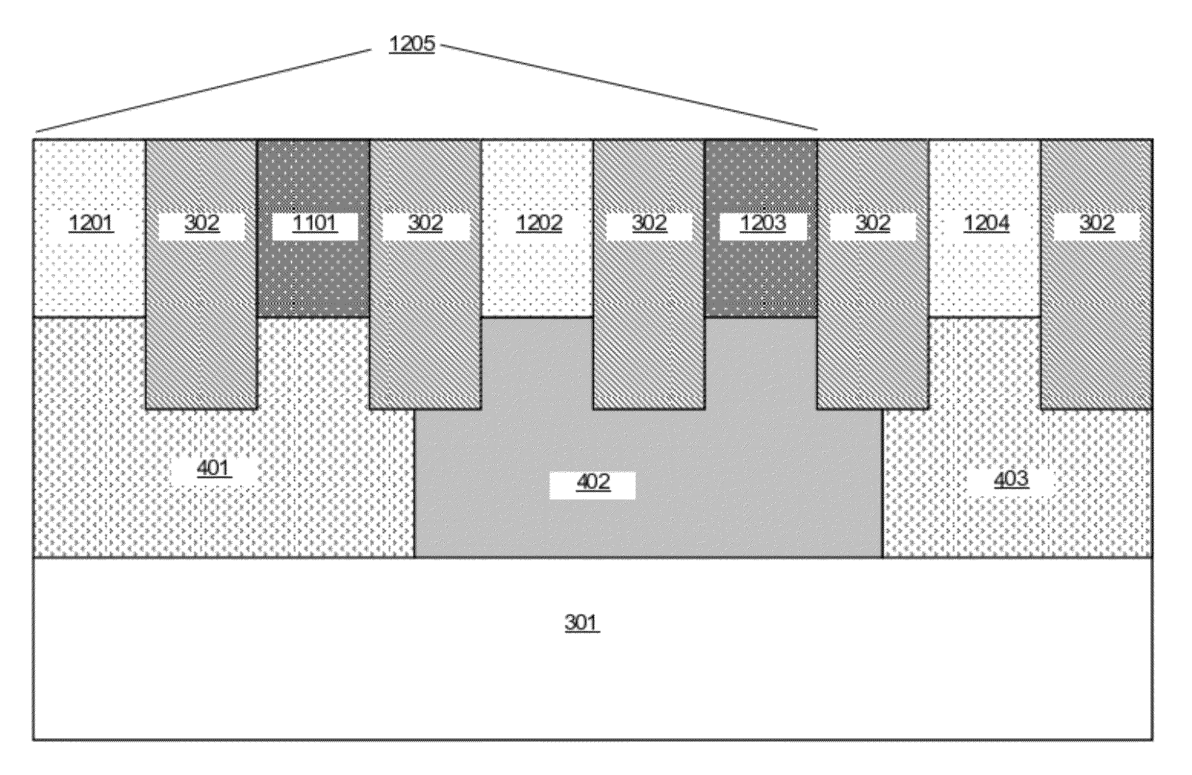
[0026]application of method 200, in which a latchup SCR with an eSiGe p+ region in the n-well is formed, begins in block 201 with formation of STI regions, n-wells and p-wells on a substrate. A substrate 301 after formation of STI regions 302 is shown in FIG. 3. Substrate 301 comprises a silicon substrate, and STI regions 302 include a dielectric material such as oxide. Then, n-well 402 and p-wells 401 and 403 are formed in the substrate 301 as is shown in FIG. 4. Formation of n-well 402 and p-wells 401 and 403 may be performed using any appropriate technique, such as implantation of the n-wells and the p-wells with appropriate respective n-type and p-type dopants, followed by a rapid thermal anneal (RTA). Then, in block 202, a junction engineering mask is applied to the IC. The junction engineering mask exposes a p+ region in any latchup SCRs on the IC, so that stressed enhanced junction engineering may be performed in the exposed p+ region. The junction engineering mask covers ESD...

second embodiment

[0028]application of method 200, in which a latchup SCR with a SiC n+ region in the p-well is formed, begins in block 201 with formation of STI regions, n-wells and p-wells on a substrate. A substrate 301 after formation of STI regions 302 is shown in FIG. 3. Substrate 301 comprises a silicon substrate, and STI regions 302 include a dielectric material such as oxide. Then, n-well 402 and p-wells 401 and 403 are formed in the substrate 301 as is shown in FIG. 4. Formation of n-well 402 and p-wells 401 and 403 may be performed using any appropriate technique, such as implantation of the n-wells and the p-wells with appropriate respective n-type and p-type dopants, followed by a rapid thermal anneal (RTA). Then, in block 202, a junction engineering mask is applied to the IC. The junction engineering mask exposes an n+ region in any latchup SCRs on the IC, so that stressed enhanced junction engineering may be performed in the exposed n+ region. The junction engineering mask covers ESD S...


PUM


Abstract

A method of forming an IC device including a latchup silicon controlled rectifier (SCR) includes forming a mask on a top surface of a substrate, wherein the mask covers a first portion of the substrate and exposes a second portion of the substrate that is located in one of an n-well and a p-well on the substrate; etching the exposed second portion of the substrate to form an etched area; forming a stress engineered junction of the latchup SCR by selective epitaxial deposition in the etched area; and removing the mask.

Description

BACKGROUND[0001]This disclosure relates generally to the field of semiconductor device fabrication, and more particularly to fabrication of integrated circuits (ICs) including silicon controlled rectifiers (SCRs), also referred to as thyristors.[0002]ICs, including complementary metal-oxide-semiconductor (CMOS) devices, are susceptible to undesired parasitic SCR action known as latchup, which if not controlled can lead to damage to the IC. Latchup describes a type of short circuit that occurs due to the existence within the CMOS circuit of parasitic SCR structures. The parasitic SCR structures comprise PNPN junctions which act as a PNP transistor and an NPN transistor cross coupled to each other. Under certain conditions, such as the presence of a transient signal, one of the PN junctions can be forward biased, which turns on the SCR. The device can remain turned on in a latchup state even after the signal which causes the forward biasing on the PN junction is removed. The two trans...

Claims


Application Information

Patent Timeline
IPC IPC(8): H01L21/332
CPCH01L29/66068H01L29/7436H01L29/66393H01L27/0248H01L29/66371H01L29/7404
Inventor CAMPI, JR., JOHN B.GAUTHIER, JR., ROBERT J.LI, JUNJUNMISHRA, RAHUL
Owner IBM CORP
Learn More