

Semiconductor circuit including electrostatic discharge circuit having protection element and trigger transistor
- Summary
- Abstract
- Description
- Claims
- Application Information
AI Technical Summary
Benefits of technology
Problems solved by technology
Method used
Image

Examples
first embodiment
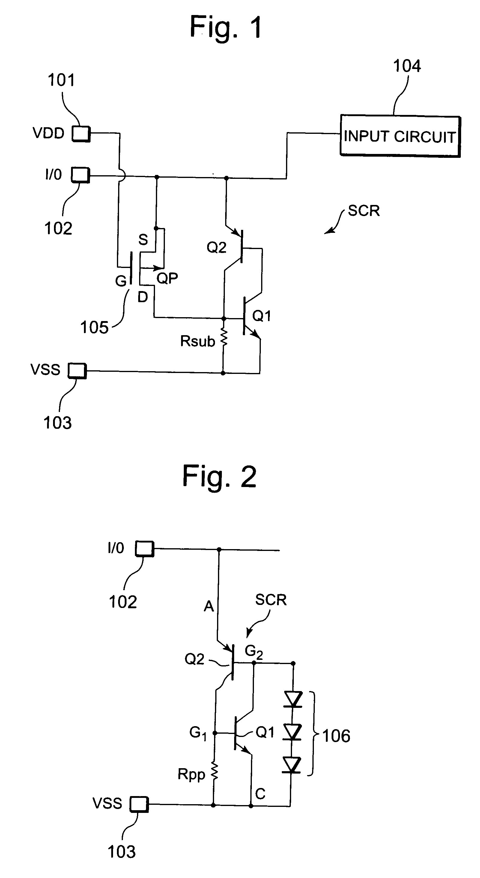
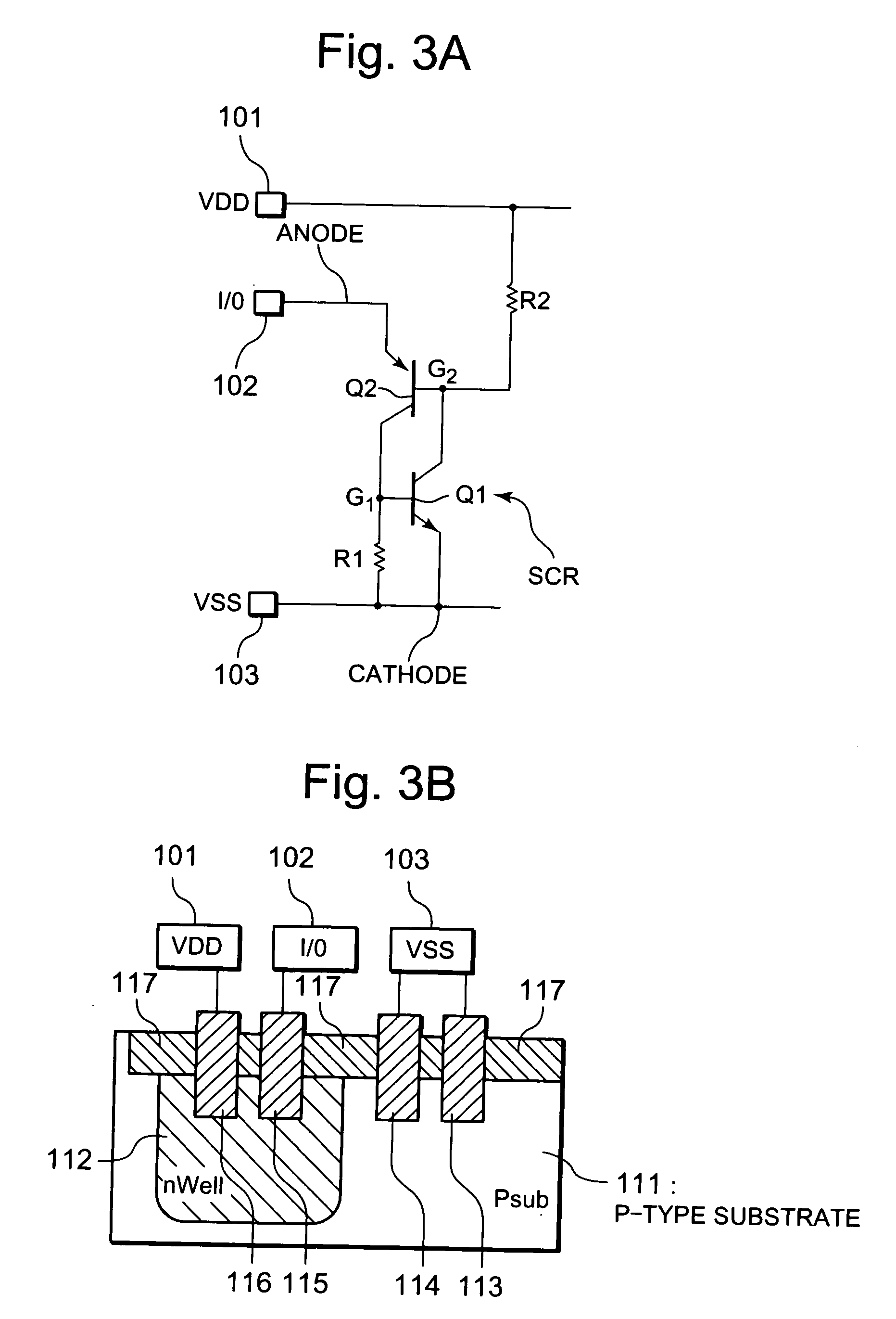
[0035]FIG. 4A is a circuit diagram for showing a configuration of the ESD protection circuit of a first embodiment of the present invention. The ESD protection circuit of the first embodiment comprises an N-gate type SCR 1, the PMOS transistor 2 for a trigger and a backward diode 3.
[0036]The SCR 1 acts as a protection element for discharging a load accumulated in the I / O pad 5 when the ESD stress (or surge) of a positive polarity is applied to the I / O pad 5. In FIG. 4A, the SCR 1 is equivalently expressed as it comprises NPN transistor Q1 and PNP transistor Q2. The anode of the SCR 1 is connected to the I / O pad 5 and its cathode is connected to the VSS pad 6. In this case, the I / O pad 5 is a pad connected to a signal line 22 for inputting or outputting a signal in respect to an internal circuit 8, and the VSS pad 6 is a pad to which the ground potential VSS is supplied from an external unit. The VSS pad 6 is connected to a VSS power supply line 23.
[0037]The PMOS transistor 2 for a t...
second embodiment
[0056]FIG. 8A is a circuit diagram for showing a configuration of the ESD protection circuit of a second embodiment of the present invention. In this embodiment, the PMOS transistor is not used, but the NMOS transistor is used as a trigger element for triggering the SCR. Along with this usage, a connecting relation among the SCR, pad and trigger element is changed from that of the first embodiment.
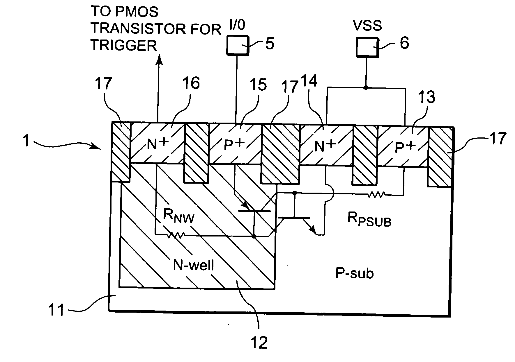
[0057]More practically, the ESD protection circuit of the second embodiment comprises an N-gate type SCR 1, the NMOS transistor 2A for a trigger, and a backward diode 3. The anode of the SCR 1 is connected to the VDD pad 4 and its cathode is connected to the I / O pad 5. The gate of the SCR 1 is connected to the drain of the NMOS transistor 2A for a trigger. The source of the NMOS transistor 2A for a trigger is connected to the I / O pad 5 and its gate and backgate are connected to the VSS pad 6.
[0058]FIG. 8B is a sectional view for showing a connected relation among the SCR 1 and each of the ...
PUM
 Abstract
Description
Claims
Application Information