Output circuit

a technology of output circuit and output circuit, which is applied in the direction of pulse technique, power conversion system, oscillation generator, etc., can solve the problems of reducing switching speed, reducing energy efficiency, and reducing the response speed of bridge circuits

Inactive Publication Date: 2013-03-05
ROHM CO LTD
View PDF6 Cites 21 Cited by
  • Summary
  • Abstract
  • Description
  • Claims
  • Application Information

AI Technical Summary

Benefits of technology

[0031]With the first low-side off-detection circuit, before the timing at which the gate signal of the low-side transistor switches from a level which instructs the low-side transistor to switch on, to a level which instructs the low-side transistor to switch off, the first bypass circuit is switched to the conduction state. In this state, the combined resistance connected to the low-side detection transistor is reduced, thereby raising the response speed. Furthermore, when the low-side transistor and the first low-side detection transistor are on, the first bypass circuit is set to a cut-off state. Thus, such an arrangement reduces a current that flows from the second terminal via the low-side detection transistor.
[0033]By employing such a first low-side off-detection circuit, such an embodiment is capable of detecting, at high speed, that the low-side transistor has switched off. Furthermore, such an arrangement reduces power consumption in the first low-side off-detection circuit.
[0038]With such an embodiment, the current that flows through the first ON transistor and the current that flows through the second ON transistor are combined, and the combined current flows through the first resistor. Thus, after the ON control signal is asserted, the voltage drop that occurs at the first terminal temporarily becomes larger, thereby accelerating the turn-on speed of the output transistor. Subsequently, the first ON transistor is turned off, and accordingly, the current that flows through the first resistor is reduced, thereby reducing the power consumption.
[0044]By providing such a clamp circuit, such an arrangement is capable of protecting the output transistor.

Problems solved by technology

However, such an arrangement has a problem of reduced energy efficiency.
Furthermore, such increased dead time leads to a problem of the bridge circuit having a reduced response speed, i.e., a problem of reduced switching speed.

Method used


Image

  • Output circuit
  • Output circuit
  • Output circuit

Examples


first embodiment

[First Embodiment]

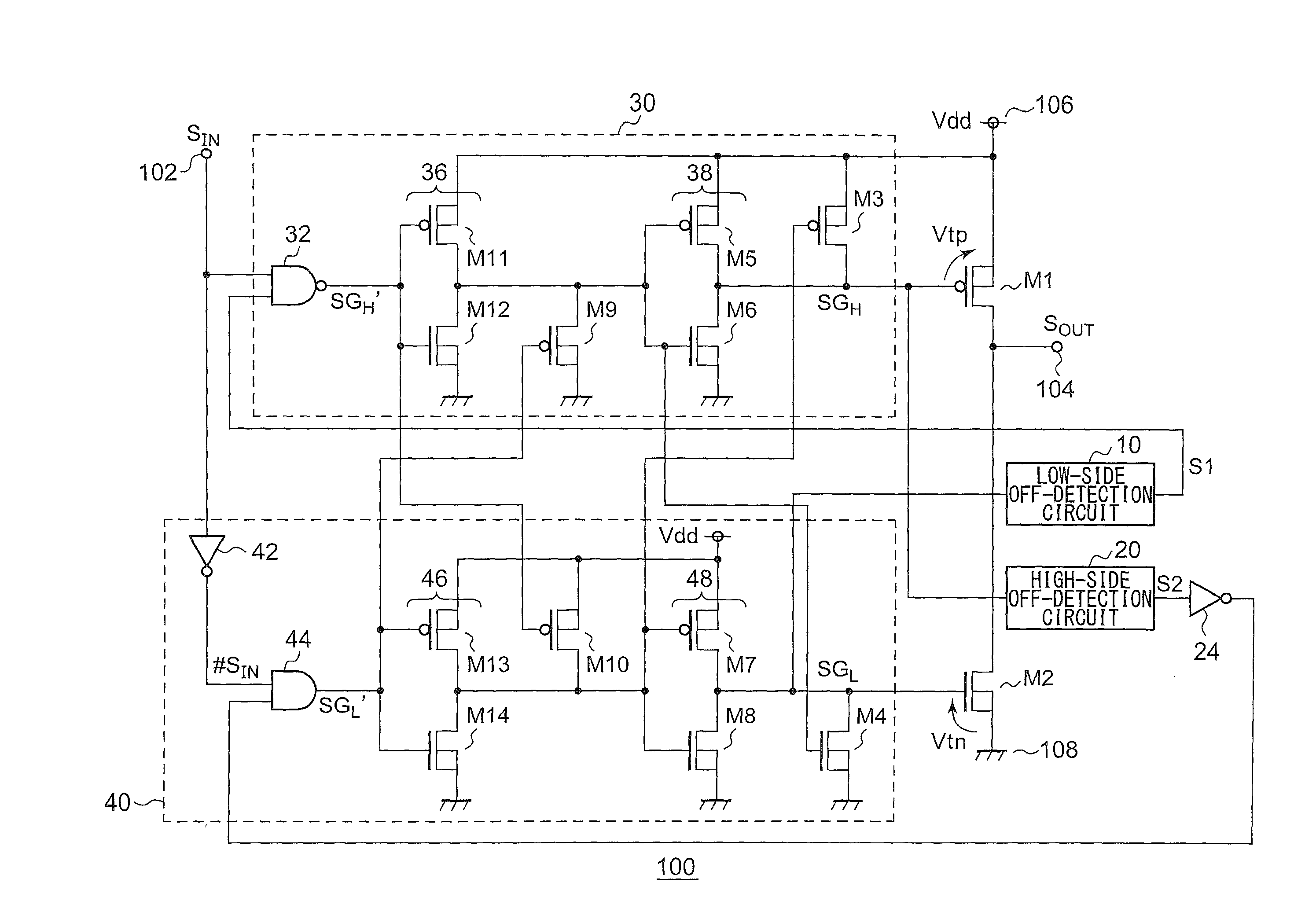
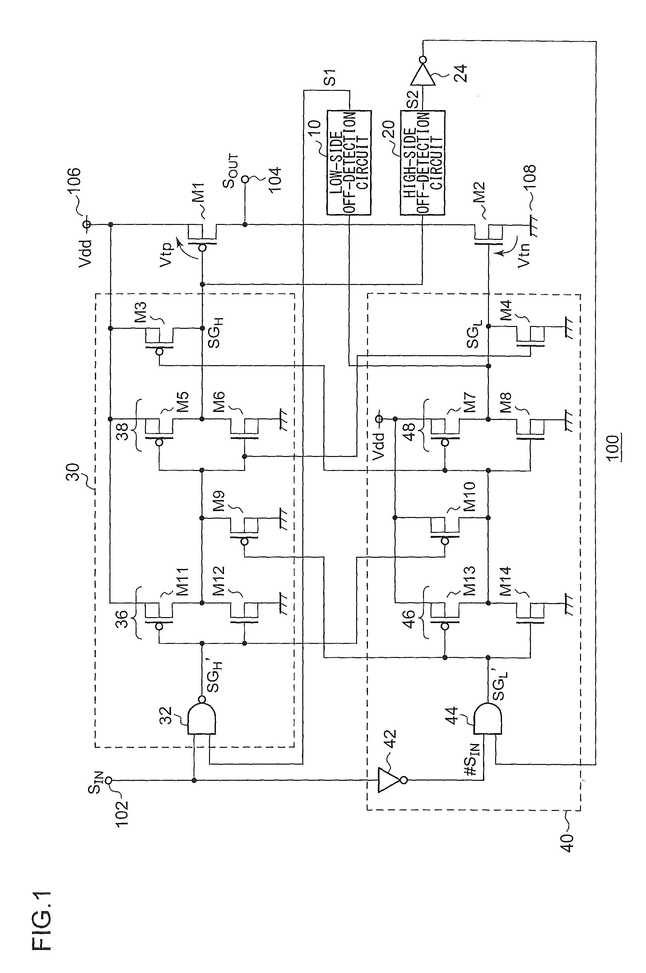
[0061]FIG. 1 is a circuit diagram which shows a configuration of a bridge output circuit 100 according to a first embodiment. The bridge output circuit 100 receives a control signal SIN via an input terminal 102, and outputs, via an output terminal 104, an output signal SOUT having a voltage level that corresponds to the level of the control signal SIN. With the present embodiment, when the control signal SIN is high level, the output signal SOUT is set to the power supply voltage Vdd, and when the control signal SIN is low level, the output signal SOUT is set to the ground voltage (0 V).

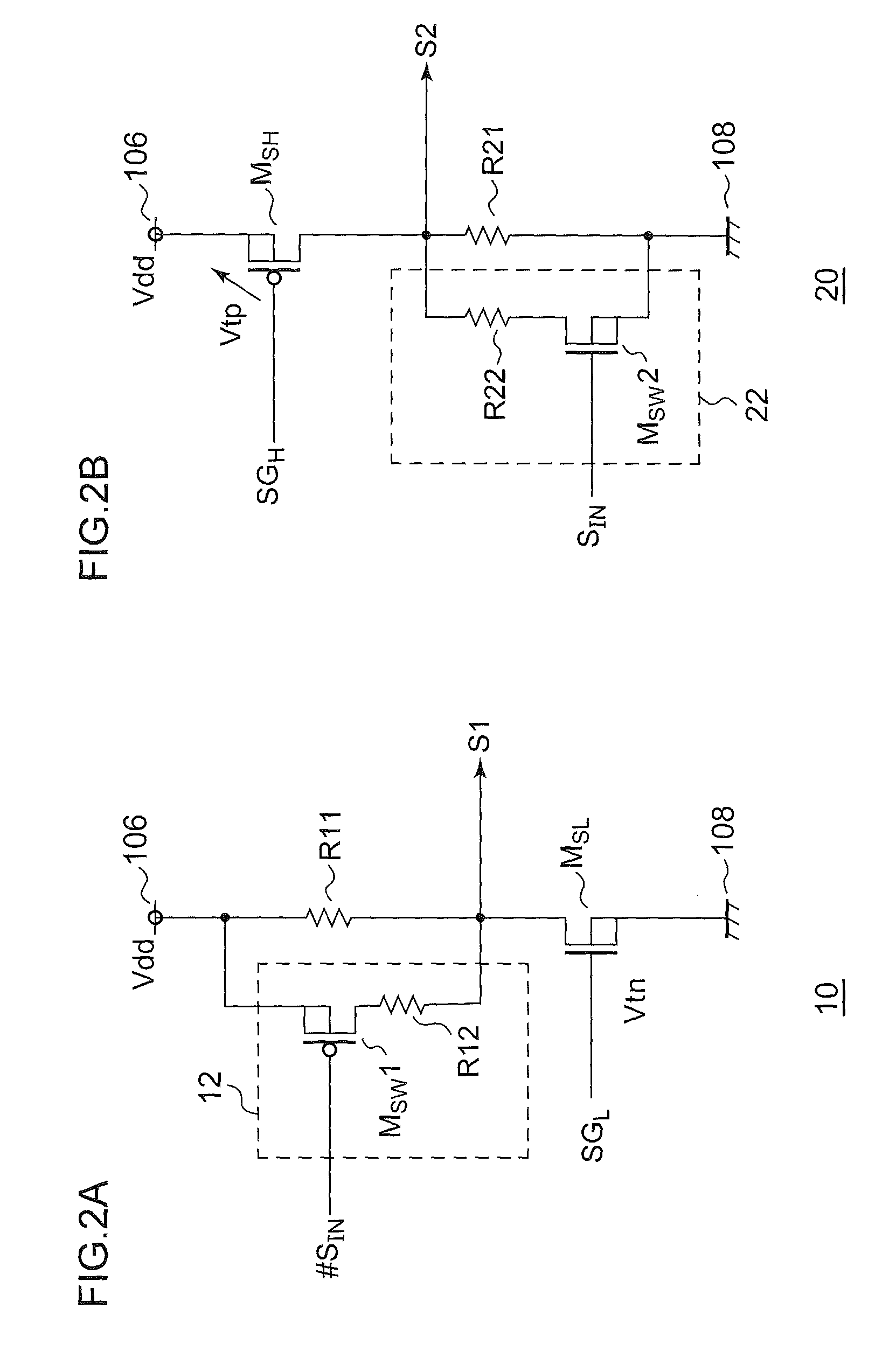
[0062]The bridge circuit 100 includes a high-side transistor M1, a low-side transistor M2, a low-side off-detection circuit 10, a high-side off-detection circuit 20, a high-side driver 30, and a low-side driver 40.

[0063]The high-side transistor M1 is arranged between a first fixed voltage terminal (power supply terminal 106) and the output terminal 104. The low-side transistor M2 i...

second embodiment

[Second Embodiment]

[0140]FIG. 8 is a circuit diagram which shows a configuration of an output circuit 100 according to a second embodiment. Via its output terminal POUT, the output circuit 100 outputs either the power supply voltage Vdd or another voltage (e.g., ground voltage) that differs from the power supply voltage Vdd, according to the levels of an on-control signal SON and an off-control signal SOFF. The output circuit 100 is a portion of a half-bridge circuit, a portion of an H-bridge circuit, or a portion of a source follower circuit.

[0141]The output circuit 100 includes: an output power transistor (which will simply be referred to as the “output transistor” hereafter) M1, a first resistor R1, a first ON circuit 110, a second ON circuit 120, an OFF circuit 130, a first clamp circuit 140, and a second clamp circuit 142. The circuit portion of the bridge output circuit 100, with the exception of the high-side transistor M1, will be referred to as a “high-side driver 30c”.

[01...


PUM


Abstract

A low-side off-detection signal compares the gate signal of a low-side transistor with a predetermined first level to generate a low-side off-detection signal indicating that the low-side transistor is off. The low-side detection transistor is of the same type as the low-side transistor, with the source connected to the ground terminal, and the gate receiving the low-side transistor gate signal. A first resistor is arranged between the drain of the low-side detection transistor and the power supply terminal. A first bypass circuit is arranged in parallel with the first resistor, and is configured to switch to the conduction state when a control signal is a level which instructs the low-side transistor to switch off, and to switch to the cut-off state when the control signal level instructs the low-side transistor to switch on. The drain signal of the low-side detection transistor is output as the low-side off-detection signal.

Description

BACKGROUND OF THE INVENTION[0001]1. Field of the Invention[0002]The present invention relates to an output circuit.[0003]2. Description of the Related Art[0004]In electronic circuits, half-bridge circuits and H-bridge circuits (which will be referred to as the “bridge output circuits” hereafter), which employ power transistors, are widely employed. The bridge output circuit includes a high-side transistor and a low-side transistor arranged in series between the power supply terminal and the ground terminal. By alternately switching on and off the high-side transistor and the low-side transistor, such an arrangement outputs either the power supply voltage or the ground voltage via a connection node that connects these two transistors.[0005]With such a bridge output circuit, if the high-side transistor and the low-side transistor are switched on at the same time, shoot-through current flows from the power supply terminal to the ground terminal. In order to prevent such a shoot-through...

Claims


Application Information

Patent Timeline
Patent Type & Authority Patents(United States)
IPC IPC(8): H03B1/00
CPCH03K17/687H02M7/5387H03K17/18H03K2217/0063
Inventor SUGIE, HISASHI
Owner ROHM CO LTD
Why Eureka
Try Eureka