Display device

a display device and display technology, applied in the field of display devices, can solve the problems of low field-effect mobility, thin film transistor deterioration, low on-state current, etc., and achieve the effects of reducing the cost of the display device, improving the display characteristics of images, and narrowing the frame of the display devi

Inactive Publication Date: 2013-03-12
SEMICON ENERGY LAB CO LTD
View PDF42 Cites 11 Cited by
  • Summary
  • Abstract
  • Description
  • Claims
  • Application Information

AI Technical Summary

Benefits of technology

[0008]Alternatively, the number of the thin film transistors included in the driver circuit is increased and an operating time of each of the thin film transistors is shortened, so that deterioration of the thin film transistors is reduced and sufficient on-state current is maintained.
[0009]As a result, in a display device whose driver circuit is formed using thin film transistors in each of which an amorphous silicon layer is used for a channel formation region, a large area occupied by the driver circuit prevents the frame of the display device from being narrowed, and thus the area of a pixel portion which is a display region is reduced.
[0013]In view of the above problems, one object of an embodiment of the present invention is to provide a display device of which manufacturing cost can be reduced and of which display characteristics of an image are excellent. Further, another object of an embodiment of the present invention is to provide a display device of which manufacturing cost can be reduced and of which frame can be narrowed.
[0020]According to the present invention, the display characteristics of an image can be improved and the cost of the display device can be reduced. Further, the frame of the display device can be narrowed, and thus, the display region of the display device can be enlarged.

Problems solved by technology

A thin film transistor in which a channel formation region is formed using an amorphous silicon layer has problems such as low field-effect mobility and low on-state current.
Further, when the thin film transistor is used for a long term, there are problems in that the thin film transistor deteriorates, the threshold voltage is shifted, and the on-state current is lowered.
On the other hand, a thin film transistor in which a channel formation region is formed using a microcrystalline silicon layer has a problem in that, whereas the field-effect mobility is higher than that of the thin film transistor using an amorphous silicon layer, the off-state current is high, and thus sufficient switching characteristics cannot be obtained.

Method used


Image

  • Display device
  • Display device
  • Display device

Examples


embodiment 1

[Embodiment 1]

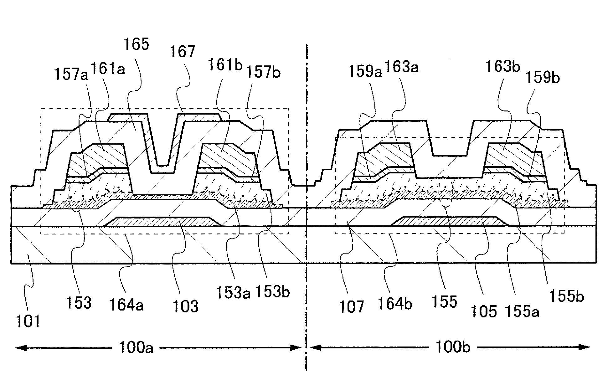
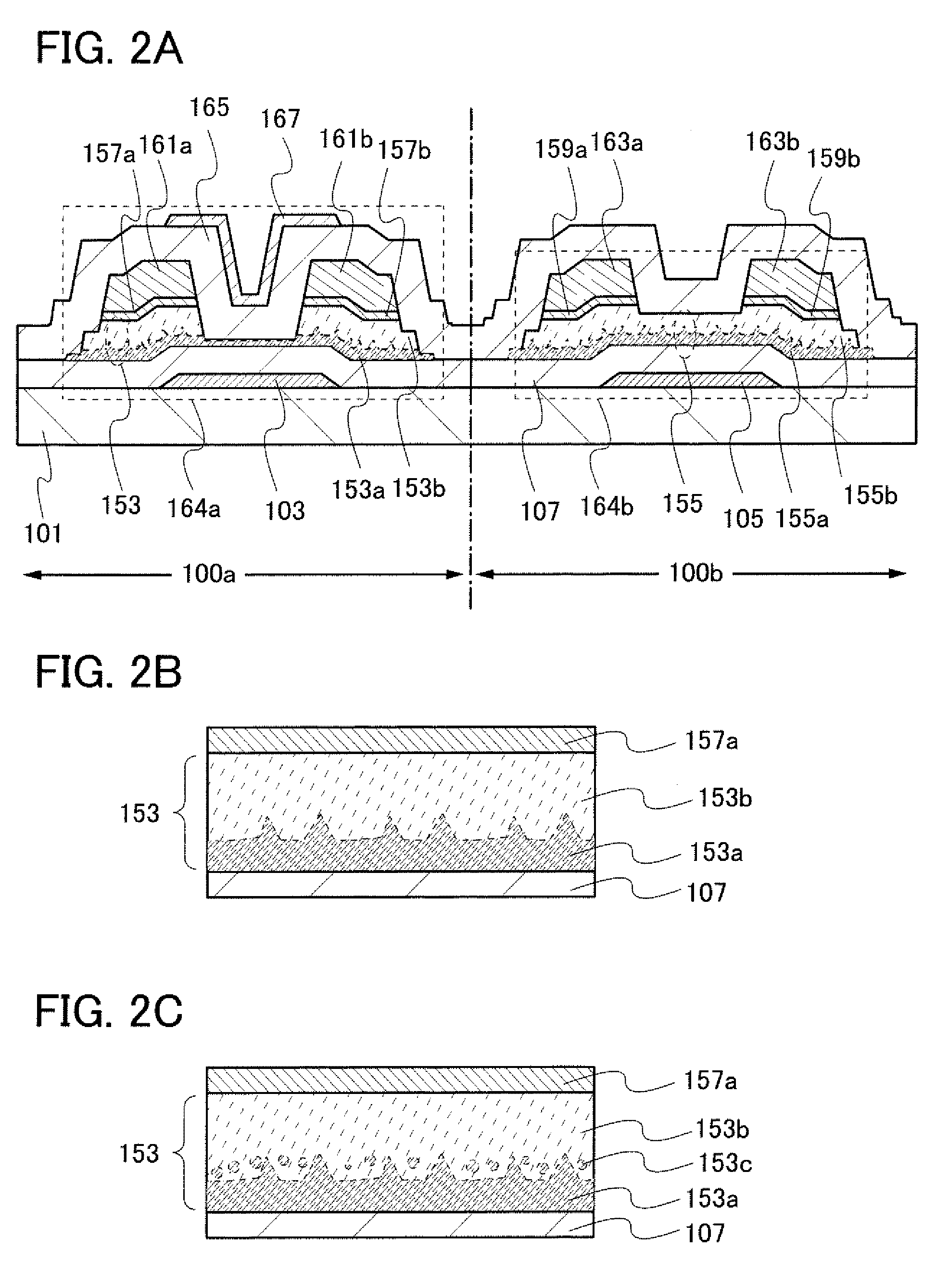
[0044]In this embodiment, a display device which is one embodiment of the present invention will be described with reference to FIGS. 1A and 1B, FIGS. 2A to 2C. FIGS. 3A to 3C, and FIG. 4. As for a thin film transistor used for a display device, an n-channel transistor has higher carrier mobility than a p-channel transistor. Further, it is preferable that all thin film transistors formed over one substrate have the same polarity because the number of manufacturing steps can be reduced. Therefore, in this embodiment. an n-channel thin film transistor will be described.

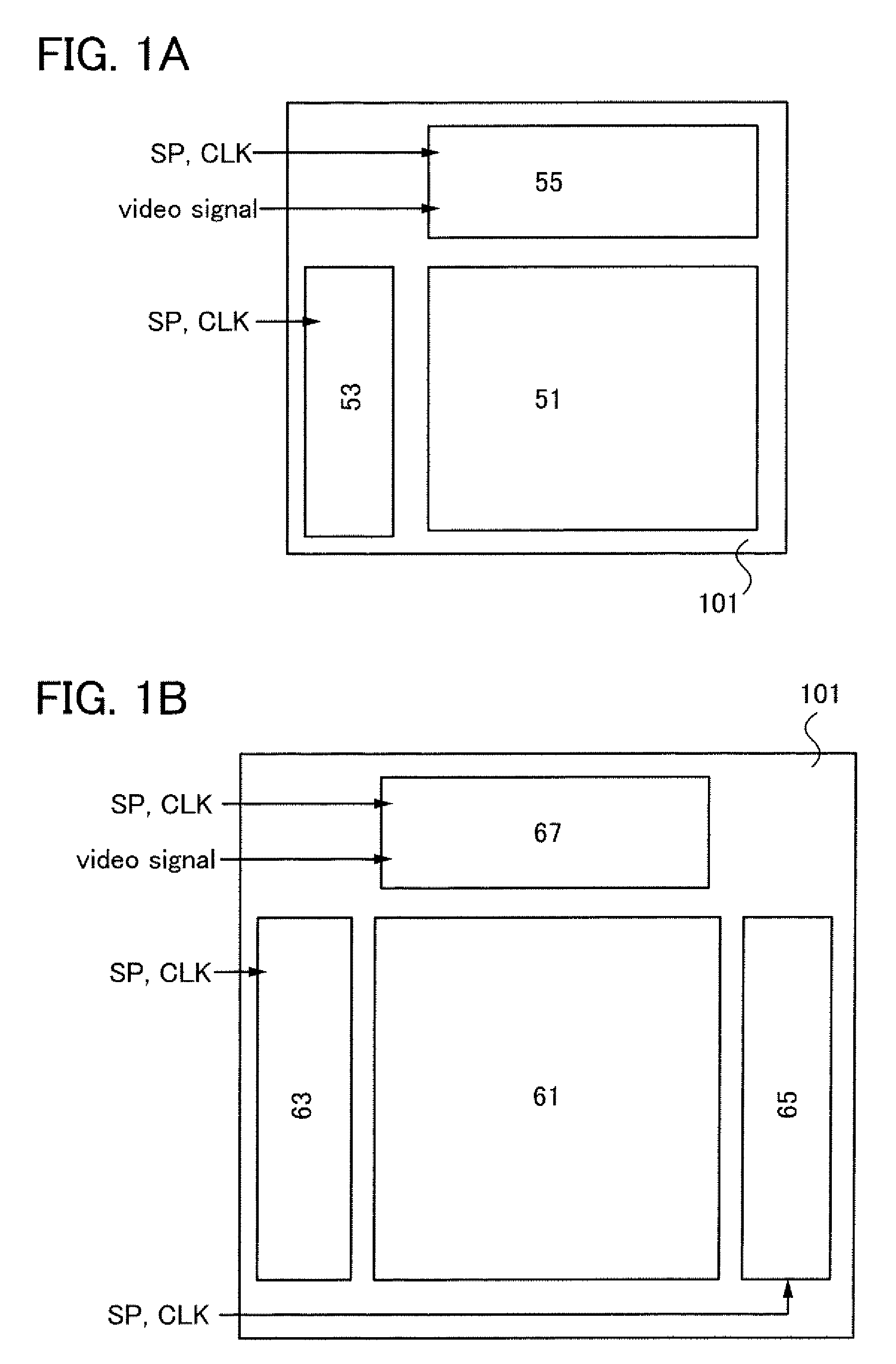
[0045]FIG. 1A is a block diagram illustrating an example of an active matrix liquid crystal display device. The liquid crystal display device illustrated in FIG. 1A includes a pixel portion 51 including a plurality of pixels each provided with a display element, a scan line driver circuit 53 controlling a scan line connected to a gate electrode of each pixel, and a signal line driver circuit 55 controlling...

embodiment 2

[Embodiment 2]

[0095]In this embodiment, a thin film transistor which is different from that described in Embodiment 1 will be described with reference to FIGS. 5A and 5B.

[0096]In FIG. 5A, a thin film transistor 178a formed in a driver circuit 100a corresponds to the thin film transistor 164a in Embodiment 1 and a thin film transistor 178b formed in a pixel portion 100b corresponds to the thin film transistor 164b in Embodiment 1. The structures other than those described hereinafter are similar to those of the thin film transistors 164a and 164b.

[0097]In the thin film transistors 178a and 178b, semiconductor layers 179 and 181 each have a stacked-layer structure in which microcrystalline semiconductor regions 179a and 181a and amorphous semiconductor regions 179b and 181b are stacked, respectively. The amorphous semiconductor regions 179b and 181b are formed using amorphous silicon.

[0098]Here, a detailed structure of the semiconductor layers 179 and 181 is described. Here, FIG. 5B ...

embodiment 3

[Embodiment 3]

[0103]In this embodiment, a thin film transistor which is different in the structure from that described in Embodiment 1 will be described with reference to FIGS. 6A and 6B.

[0104]In FIG. 6A, a thin film transistor 174a formed in a driver circuit 100a corresponds to the thin film transistor 164a in Embodiment 1 and a thin film transistor 174b formed in a pixel portion 100b corresponds to the thin film transistor 164b in Embodiment 1.

[0105]In the thin film transistors 174a and 174b, each end portions of semiconductor layers 153 and 155 are positioned not outside gate electrodes 175 and 177 but over the gate electrodes 175 and 177, with a gate insulating layer 107 provided therebetween. With the structure of the thin film transistors 174a and 174b, in a display device including a backlight such as a liquid crystal display device, the gate electrodes 175 and 177 each serve as a light-blocking member with respect to light delivered to the semiconductor layers 153 and 155; t...


PUM


Abstract

An object is to provide a display device whose frame can be narrowed and whose display characteristics are excellent. The display device includes a driver circuit and a pixel portion. The driver circuit and the pixel portion are formed using a dual-gate thin film transistor and a single-gate thin film transistor, respectively. In the dual-gate thin film transistor in the display device, a semiconductor layer is formed using a microcrystalline semiconductor region and a pair of amorphous semiconductor regions, and a gate insulating layer and an insulating layer are in contact with the microcrystalline semiconductor region of the semiconductor layer.

Description

BACKGROUND OF THE INVENTION[0001]1. Field of the Invention[0002]The present invention relates to a display device having an inverted staggered thin film transistor in each of a driver circuit and a pixel portion.[0003]2. Description of the Related Art[0004]As one kind of field-effect transistor. a thin film transistor in which a channel formation region is formed using a semiconductor layer formed over a substrate having an insulating surface is known. Techniques in which amorphous silicon, microcrystalline silicon. or polycrystalline silicon is used for the semiconductor layer used in the thin film transistor have been disclosed. A typical application example of the thin film transistor is a liquid crystal display television device, in which the thin film transistor has been put to practical use as a switching transistor for each pixel that constitutes a display screen.[0005]Further, there is a display device in which the number of external components is reduced and thin film trans...

Claims


Application Information

Patent Timeline
Patent Type & Authority Patents(United States)
IPC IPC(8): H01L29/04
CPCH01L27/1233H01L27/1251H01L29/78696H01L29/04H01L27/1288H01L29/78648
Inventor MIYAIRI, HIDEKAZUISA, TOSHIYUKI
Owner SEMICON ENERGY LAB CO LTD
Why Eureka
Try Eureka