Display device

a display device and display technology, applied in static indicating devices, instruments, transportation and packaging, etc., can solve the problems of low field-effect mobility and a small current, deterioration of thin film transistors, and shift of threshold voltages, so as to improve the display characteristics of images, reduce the cost of display devices, and narrow the frame of display devices

Inactive Publication Date: 2010-04-01
SEMICON ENERGY LAB CO LTD
View PDF27 Cites 45 Cited by
  • Summary
  • Abstract
  • Description
  • Claims
  • Application Information

AI Technical Summary

Benefits of technology

[0022]According to the present invention, the display characteristics of an image can be improved while the cost of the display device can

Problems solved by technology

The thin film transistor in which an amorphous silicon layer is used for forming a channel formation region has problems such as a low field-effect mobility and a small on current.
Further, when the thin film transistor is used for a long-term, there are problems in that the thin film transistor is deteriorated, the threshold voltage is shifted, and on curre

Method used


Image

  • Display device
  • Display device
  • Display device

Examples


embodiment 1

[0053]In this Embodiment, a display device that is one embodiment of the present invention will be described with reference to a block diagram and the like.

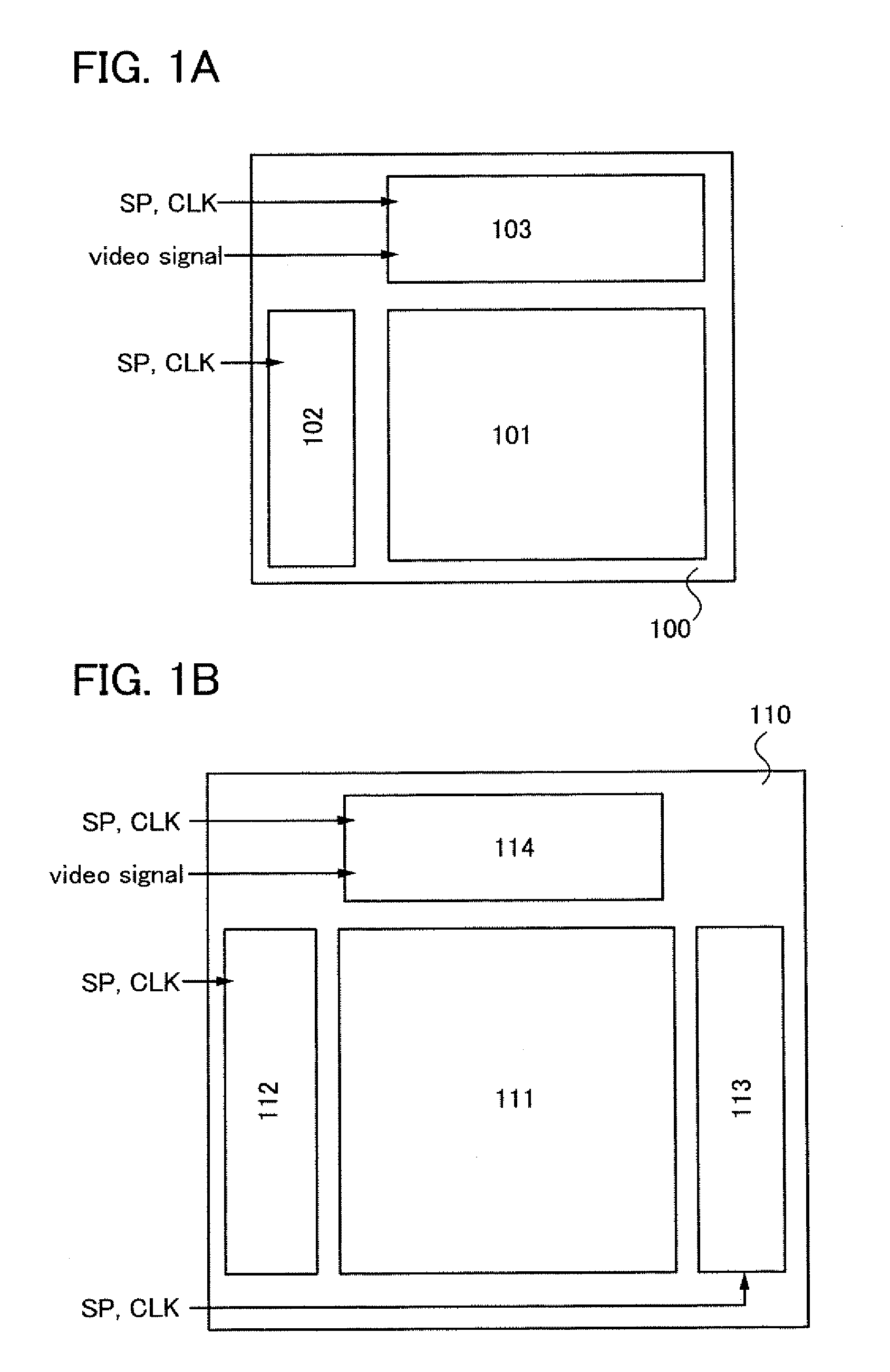
[0054]FIG. 1A illustrates an example of a block diagram of an active matrix liquid crystal display device. The liquid crystal display device illustrated in FIG. 1A includes a pixel portion 101 including a plurality of pixels each provided with a display element, a scan line driver circuit 102 controlling a scan line connected to a gate electrode of each pixel, and a signal line driver circuit 103 controlling a video signal input to a selected pixel over a substrate 100.

[0055]FIG. 1B illustrates an example of a block diagram of an active matrix light-emitting display device to which the present invention is applied. The light-emitting display device illustrated in FIG. 1B includes a pixel portion 111 including a plurality of pixels each provided with a display element, a first scan line driver circuit 112 and a second scan line dr...

embodiment 2

[0066]In this Embodiment, circuit diagrams of driver circuits of the display device described in Embodiment 1 will be described with reference to FIG. 3, FIG. 4, FIG. 5, and FIG. 6.

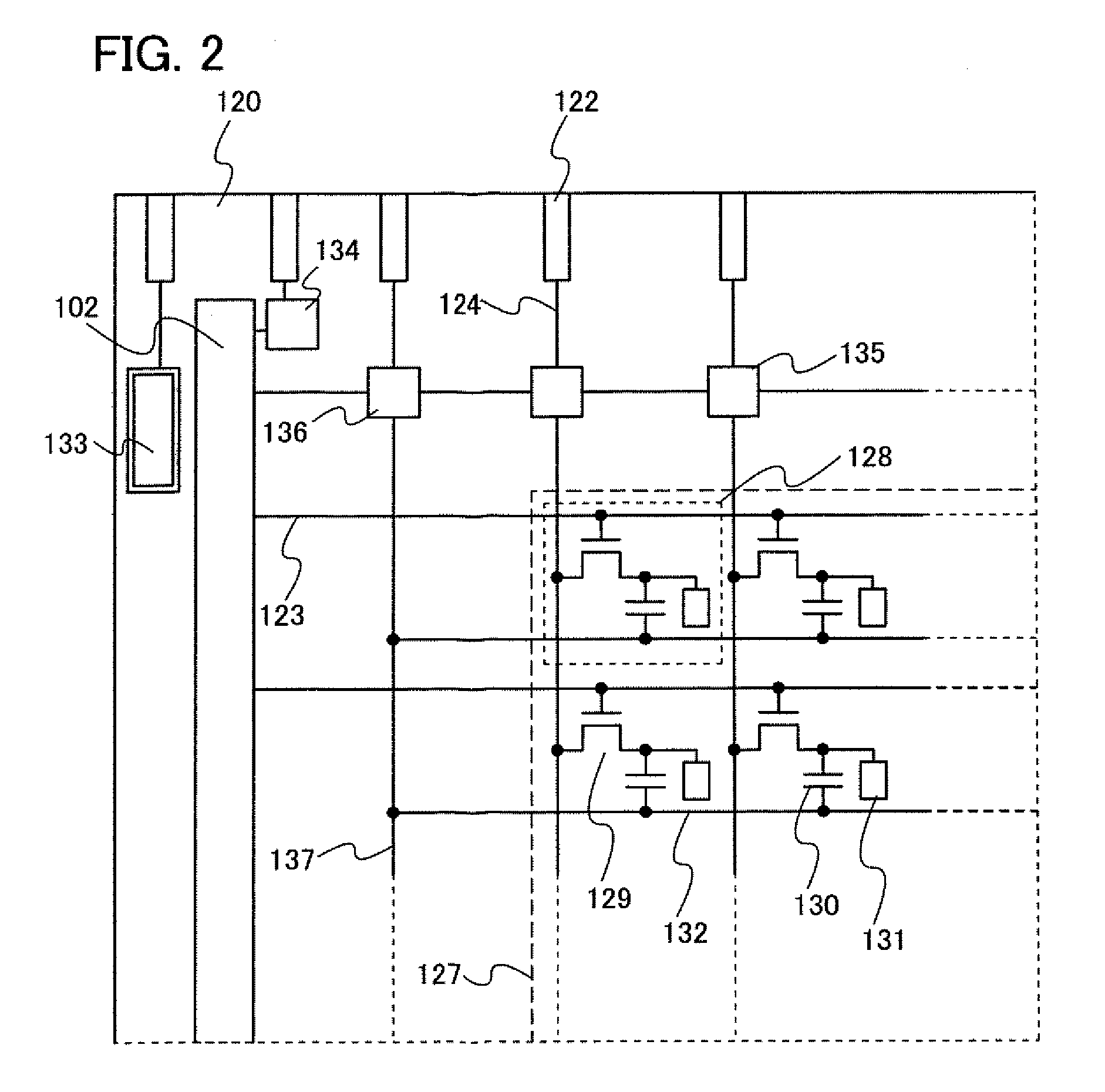
[0067]First, a shift register circuit included in the scan line driver circuit shown in Embodiment 1 will be described.

[0068]The shift register circuit illustrated in FIG. 3 includes a plurality of flip-flop circuits 201, control signal lines 202, 203, 204, 205, and 206, and reset lines 207.

[0069]As in the shift register circuit illustrated in FIG. 3, a start pulse SSP is inputted to an input terminal IN of the flip-flop circuit 201 of the first stage through the control signal line 202. An output signal terminal Sout of the flip-flop circuit 201 of the previous stage is connected to an input terminal IN of the flip-flop circuit 201 of the subsequent stages. A reset terminal RES of the N-th stage (N is a natural number) is connected to the output signal terminal Sout of the flip-flop circuit of the (N+3-t...

embodiment 3

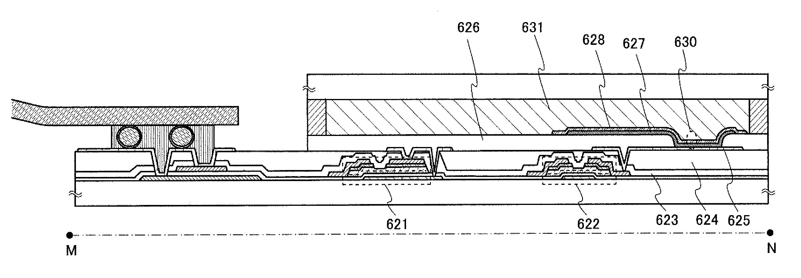
[0105]In this Embodiment, as to the display device described in Embodiments 1 and 2, structures of the logic circuit portion, the switch portion, and the thin film transistor in the pixel portion will be described. As for a thin film transistor used for a display device, an n-type transistor has higher carrier mobility than a p-type transistor. It is preferable that all thin film transistors formed over the same substrate have the same polarity because the number of manufacturing steps can be reduced. In this Embodiment, an n-type thin film transistor will be described.

[0106]FIG. 7 and FIG. 8A each illustrate a cross-sectional view of one mode (structure 1) of a logic circuit portion 391, a switch portion 393, and a pixel portion 395 in the display device according to this Embodiment.

[0107]An EDMOS circuit is used for the logic circuit portion 391 in the display device illustrated in FIG. 7. One of a depletion type TFT and an enhancement type TFT in the EDMOS circuit is a dual-gate ...


PUM


Abstract

A display device of which frame can be narrowed and of which display characteristics are excellent is provided. In a display device including a switch portion or a buffer portion, a logic circuit portion, and a pixel portion, the pixel portion includes a first inverted staggered TFT and a pixel electrode which is connected to a wiring of the first inverted staggered TFT, the switch portion or the buffer portion includes a second inverted staggered TFT in which a first insulating layer, a semiconductor layer, and a second insulating layer are interposed between a first gate electrode and a second gate electrode, the logic circuit portion includes an inverter circuit including a third inverted staggered thin film transistor and a fourth inverted staggered thin film transistor, and the first to the fourth inverted staggered thin film transistors have the same polarity. The inverter circuit may be an EDMOS circuit.

Description

BACKGROUND OF THE INVENTION[0001]1. Field of the Invention[0002]The present invention relates to a display device having an inverted staggered thin film transistor in each of a driver circuit and a pixel portion.[0003]2. Description of the Related Art[0004]As one kind of field-effect transistors, a thin film transistor in which a channel formation region is formed in a semiconductor layer formed over a substrate having an insulating surface is known. Techniques in which amorphous silicon, microcrystalline silicon, or polycrystalline silicon is used for semiconductor layers used in thin film transistors have been disclosed. A typical application of a thin film transistor is a liquid crystal television device in which the thin film transistor has been put to the practical use as a switching transistor for each pixel included in a display panel.[0005]Further, for reduction of the cost of a display device, there is a display device of which the number of external components is reduced a...

Claims


Application Information

Patent Timeline
IPC IPC(8): G06F3/038H01L33/00
CPCH01L27/1214H01L27/1251Y10T428/24331H01L29/78648H01L29/04H01L27/1229H01L27/1255G02F1/1368G02F1/1365G02F1/133345G02F1/134363G02F1/13439
Inventor YAMAZAKI, SHUNPEIOSADA, TAKESHIMIYAIRI, HIDEKAZUJINBO, YASUHIRO
Owner SEMICON ENERGY LAB CO LTD
Why Eureka
Try Eureka