Epitaxial substrate for electronic device and method of producing the same

a technology of electronic devices and substrates, applied in the direction of crystal growth process, polycrystalline material growth, chemically reactive gases, etc., can solve the problems of depletion layer not expanding efficiently, power consumption increase, loss, etc., to enhance withstand voltage, and reduce lateral leakage current

Active Publication Date: 2013-04-02
DOWA ELECTRONICS MATERIALS CO LTD
View PDF16 Cites 5 Cited by
  • Summary
  • Abstract
  • Description
  • Claims
  • Application Information

AI Technical Summary

Benefits of technology

[0019]The epitaxial substrate for an electronic device of the present invention has a buffer including an initially grown layer made of an AlN material and a predetermined superlattice laminate, a predetermined main laminated body on the buffer, and both of the superlattice laminate and a portion on the buffer side of the main laminated body has carbon concentration of 1×10¹⁸ / cm3 or higher. Accordingly, it is possible not only to make decrease in lateral leakage current and achievement of good properties of withstand voltage in a lateral direction compatible but also enhance withstand voltage in the vertical direction.
[0020]Further, since the epitaxial substrate for an electronic device of the present invention has a buffer including an initially grown layer made of an AlN material and a predetermined superlattice laminate, a predetermined main laminated body on the buffer, and both of the superlattice laminate and a portion on the buffer side of the main laminated body has carbon concentration of 1×10¹⁸ / cm3 or higher, it is possible to produce an epitaxial substrate for an electronic device capable of making decrease in lateral leakage current and achievement of good properties of withstand voltage in a lateral direction compatible, as well as enhancing withstand voltage in the vertical direction.
[0021]Yet further, the Si single crystal substrate has specific resistance of 1000 Ω·cm or higher; total maximum concentrations of group III atoms in a portion of the Si single crystal substrate, from the interface between the substrate and the initially grown layer to 0.1 μm depth of the substrate, is 1×10¹⁶ / cm3 or lower; and total concentrations of group III atoms the Si single crystal substrate, at a position from the interface between the substrate and the initially grown layer to 0.3 μm depth of the substrate, is 1×10¹⁵ / cm3 or lower in the epitaxial substrate for an electronic device of the present invention, whereby an effect of decreasing loss when the electronic device is operated at a relatively high frequency can also be obtained in addition to the aforementioned superior effects.
[0022]Yet further, the Si single crystal substrate is formed to have: specific resistance of 1000 Ω·cm or higher; total maximum concentrations of group III atoms of 1×10¹⁶ / cm3 or lower in a portion thereof from the interface between the substrate and the initially grown layer to 0.1 μm depth of the substrate; and total concentrations of group III atoms of 1×10¹⁵ / cm3 or lower at a position thereof from the interface between the substrate and the initially grown layer to 0.3 μm depth of the substrate in the present invention, whereby an effect of producing an epitaxial substrate for an electronic device capable of decreasing loss when the electronic device is operated at a relatively high frequency can also be obtained in addition to the aforementioned superior effects.

Problems solved by technology

Increase in leakage current results in increase in power consumption, possibly causing problems such as heat generation.
This loss occurs because, in a case where electric charge exists in a substrate or an epitaxial film thereon, a depletion layer fails to expand efficiently and the charge causes capacitive or inductive interactions with an electrode provided on a surface of the substrate.
However, in the invention disclosed in JP 2007-251144, there arises a problem in that, since a GaN-based low temperature buffer layer is employed when a group III nitride layer is grown on a substrate, a through-defect such as a pit is generated in a case where the substrate uses Si due to a reaction between Si and Ga, possibly deteriorating withstand voltage in the vertical direction.
Yet further, JP 2003-282598 and JP 2008-522447, which consider neither withstand voltage in the vertical direction nor withstand voltage of the buffer layer, cannot ensure sufficient withstand voltage in the vertical direction when applied to a semiconductor substrate such as a Si substrate.

Method used


Image

  • Epitaxial substrate for electronic device and method of producing the same
  • Epitaxial substrate for electronic device and method of producing the same
  • Epitaxial substrate for electronic device and method of producing the same

Examples


example 1

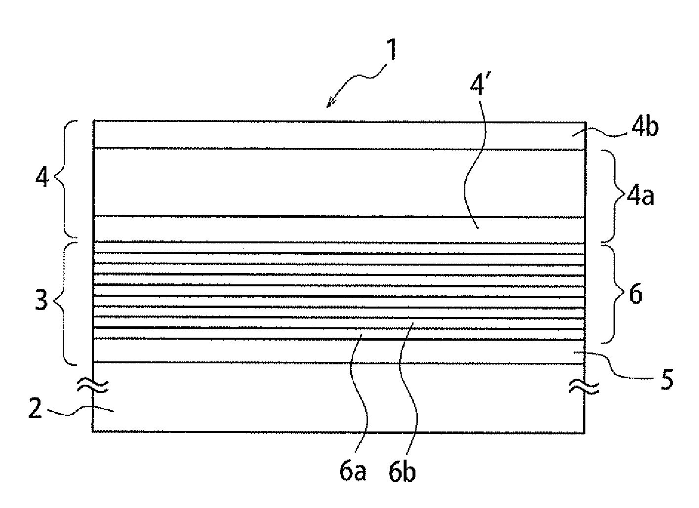
[0053]An initially grown layer (AlN material with 100 nm thickness) and a superlattice laminate (totally 85 layers of AlN with 4 nm film thickness and Al0.15 Ga0.85N with 25 nm film thickness) were grown on each of (111) faces of 4 inch Si single crystal substrates having 600 μm thickness and specific resistance values of 1×10⁻¹ Ω·cm, 1×10 Ω·cm, 2×10³ Ω·cm and 1×10⁴ Ω·cm, respectively, to form buffer layers, followed by epitaxial growth of a channel layer (GaN material with 1.5 μm thickness) and an electron supply layer (Al0.25 Ga0.75N material with 20 nm thickness) on each of the buffer layers to form a main laminated body having a HEMT structure, whereby Samples 1 to 4 were obtained. Carbon concentrations of the superlattice laminates of these Samples were varied. Carbon concentration of a portion, on the buffer side, of each of the main laminated bodies of the Samples was within the range of 1.5 to 2.0×10¹⁸ / cm3. Carbon concentration of a portion, on the electron supply layer side...

example 2

[0055]Sample 5 was prepared by substantially the same method as Sample 2 of Example 1, except that the initially grown layer was formed by a GaN material (thickness: 20 nm) which grew at 700° C. and conditions of growth temperatures and growth pressures of the respective layers were set as shown in Table 2.

[0056]

TABLE 2GrowthGrowthLayerpressure (kPa)temperature (C. °)Initially grown layer10700Superlattice laminateP1 (1-120)1025Channel layer on buffer side101025Channel layer on electron 1001075supply layer sideElectron supply layer101025

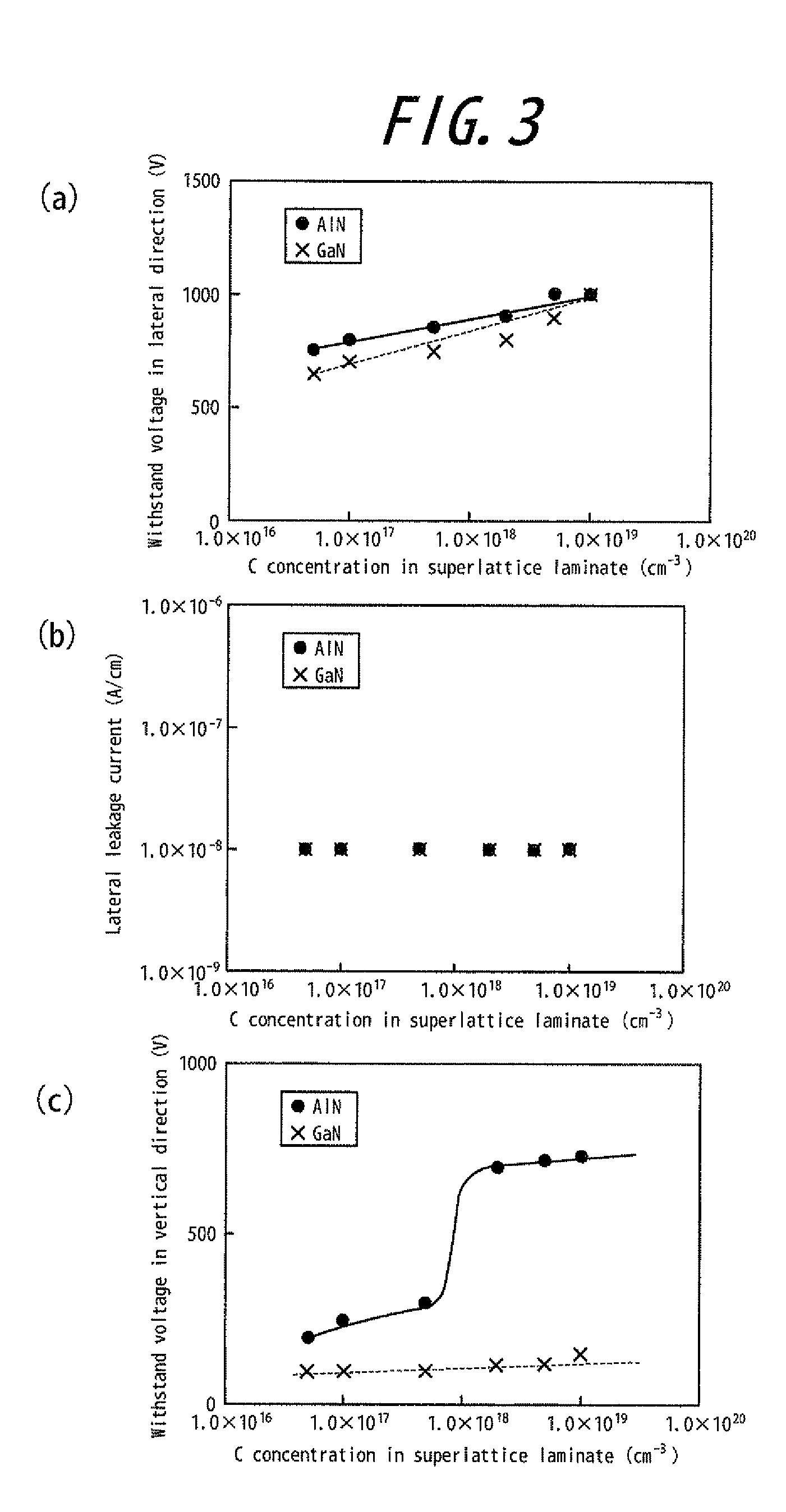
[0057]FIG. 3(a), FIG. 3(b) and FIG. 3(c) show measurement results of withstand voltage in lateral direction, lateral leakage current, and withstand voltage in vertical direction of Sample 2 and Sample 5, respectively. The measurement was carried out as follows.

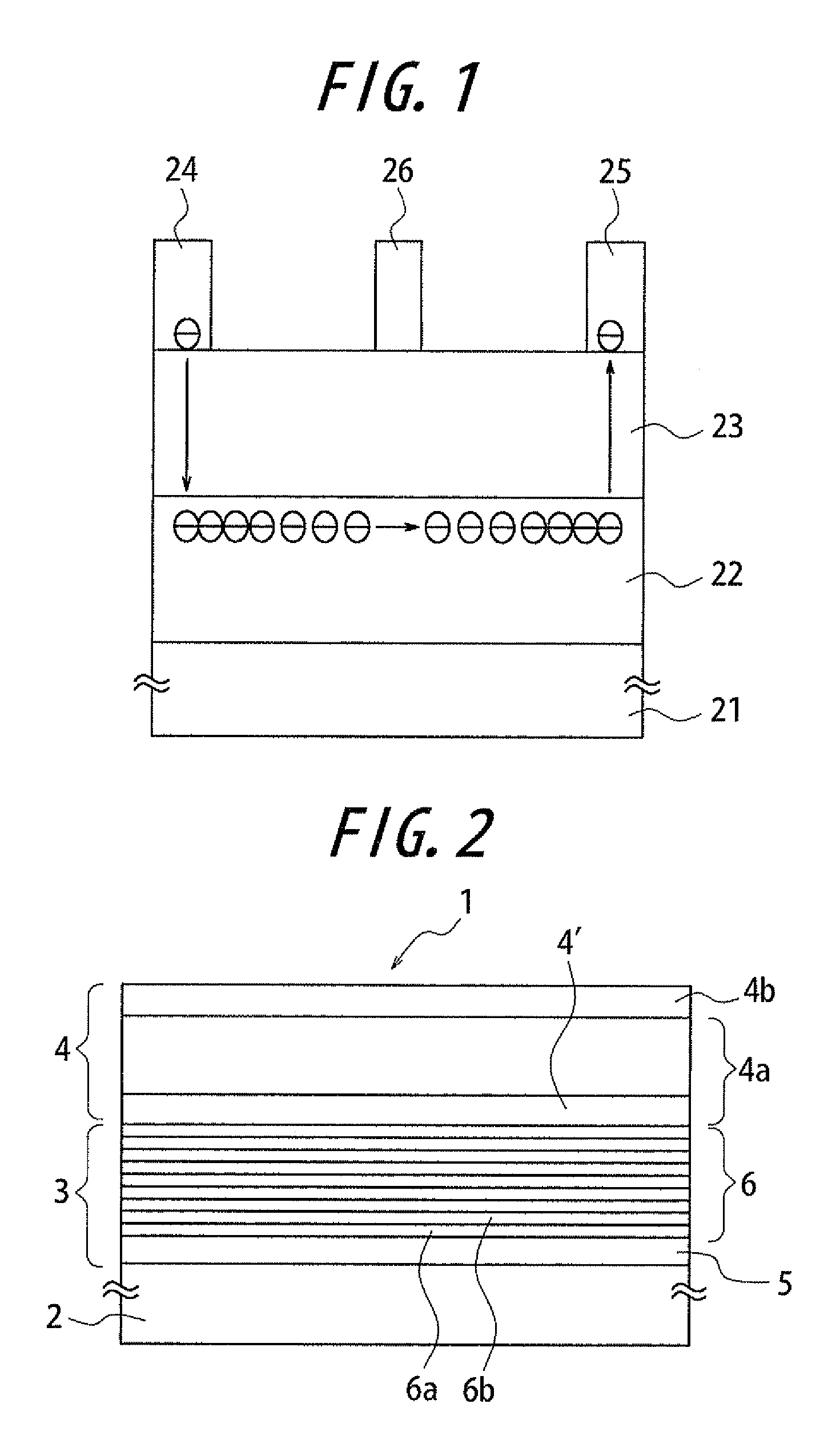
[0058]Withstand voltage in vertical direction is measured by: forming on a surface of a substrate ohmic electrodes each having a Ti / Al laminate structure (80 μmφ); etching the outer side of each...

example 3

[0062]Samples 6 to 9 were prepared by substantially the same method as Samples 1 to 4 of Example 1, except that growth pressure for the superlattice laminate was set 10 kPa, the carbon concentration of a portion on the buffer side of the main laminated body was varied, and conditions of growth temperatures and growth pressures of the respective layers were set as shown in Table 3. The carbon concentration of the superlattice laminate was adjusted by changing growth pressure P2 shown in Table 3, for example, by decreasing film-forming pressure to increase carbon concentration therein. The carbon concentration of each of the superlattice bodies of Samples 6-9 was within the range of 1.5 to 2.5×10¹⁸ / cm3.

[0063]

TABLE 3GrowthGrowthLayerpressure (kPa)temperature (C. °)Initially grown layer10700Superlattice laminate101025Channel layer on buffer sideP2 (1-120)1025Channel layer on electron 1001075supply layer sideElectron supply layer101025

[0064]FIG. 4(a), FIG. 4(b) and FIG. 4(c) show measure...


PUM


Abstract

An epitaxial substrate for an electronic device having a Si single crystal substrate, a buffer as an insulating layer formed on the Si single crystal substrate, and a main laminated body formed by plural group III nitride layers epitaxially grown on the buffer, wherein a lateral direction of the epitaxial substrate is defined as an electric current conducting direction. The buffer including at least an initially grown layer in contact with the Si single crystal substrate and a superlattice laminate constituted of a superlattice multilayer structure on the initially grown layer.

Description

TECHNICAL FIELD[0001]The present invention relates to an epitaxial substrate for an electronic device and a method of producing the same, in particular, to an epitaxial substrate for HEMT and a method of producing the same.PRIOR ART[0002]In recent years, HEMT (High electron mobility transistor) has been widely used as high-speed FET (Field effect transistor) as speed required of an IC device increases. Such a FET-type transistor as described above is generally formed, as schematically illustrated in FIG. 1, for example, by laminating a channel layer 22 and an electron supply layer 23 on a substrate 21 and then providing a surface of the electron supply layer 23 with a source electrode 24, a drain electrode 25 and a gate electrode 26. When this transistor device is operated, electrons are moved through the source electrode 24, the electron supply layer 23, the channel layer 22, the electron supply layer 23 and the drain electrode 25 in this order, thereby defining the lateral directi...

Claims


Application Information

Patent Timeline
Patent Type & Authority Patents(United States)
IPC IPC(8): H01L29/06
CPCC30B25/18C30B29/403C30B29/406H01L21/02381H01L21/02458H01L29/155H01L21/0254H01L21/0262H01L29/1075H01L29/66462H01L29/7787H01L21/02507H01L21/20H01L29/778
Inventor IKUTA, TETSUYASHIMIZU, JOSHIBATA, TOMOHIKO
Owner DOWA ELECTRONICS MATERIALS CO LTD
Why Eureka
Try Eureka